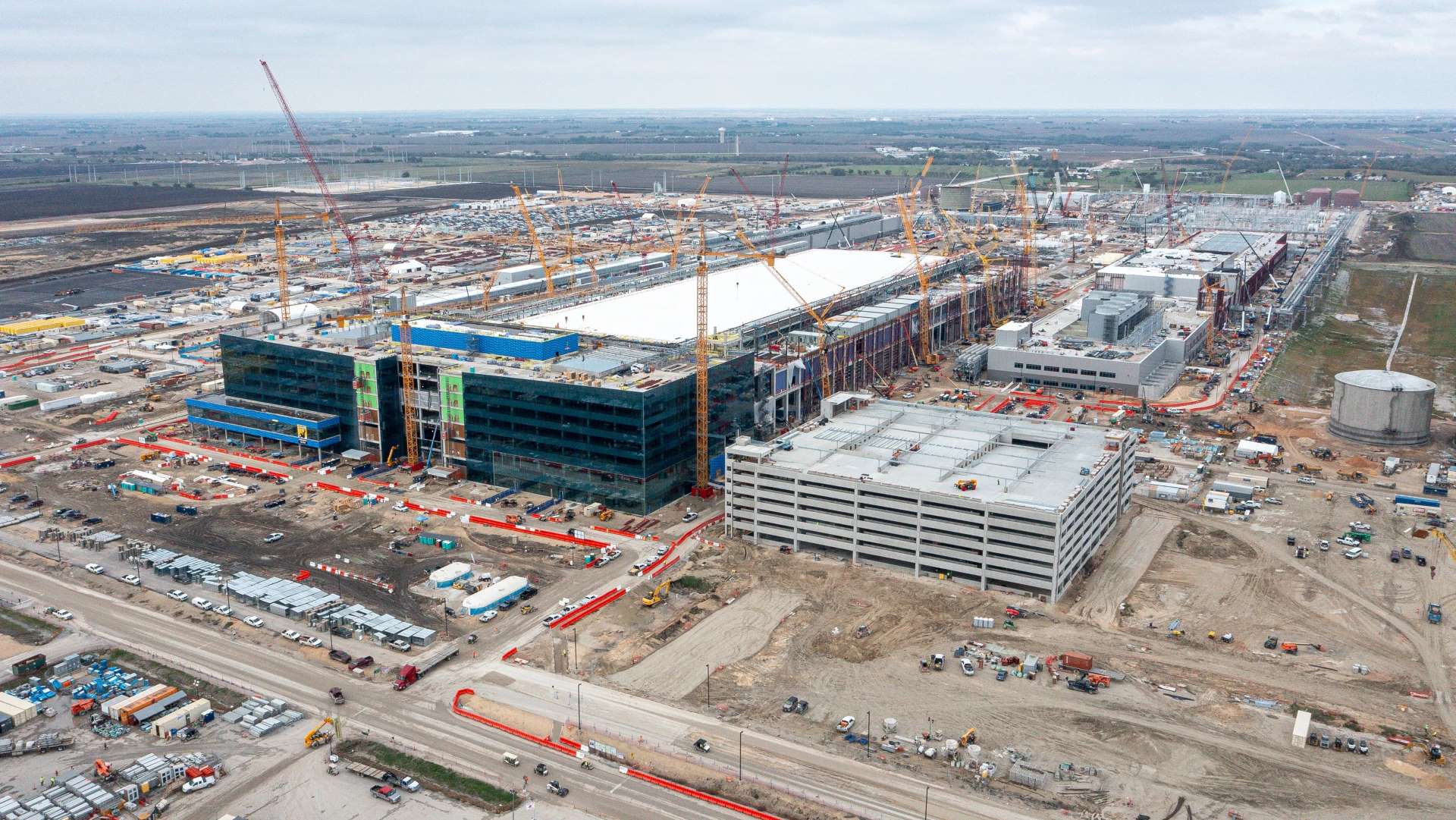
Samsung is making a bold play in the U.S. semiconductor market, and it could reshape the competition in advanced chip manufacturing. With TSMC still firmly opposed to bringing its most cutting-edge chipmaking technology onto U.S. soil, Samsung has a rare opening to claim center stage in America with its next-generation 2nm GAA process. That push is expected to run through Samsung’s Taylor, Texas plant, where operations are slated to begin soon.
Behind the scenes, the Taylor facility has already been preparing for advanced production. Reports previously pointed to ASML staff helping set up EUV lithography equipment, a critical ingredient for manufacturing sub-5nm chips at higher yields. EUV tools are essential for modern leading-edge nodes, helping improve both efficiency and output consistency as chip features shrink further.
What’s changed is Samsung’s direction at Taylor. While the plant had been associated with ramping up 4nm manufacturing—largely because 4nm can be easier to stabilize at strong yield levels—the latest information suggests Samsung has shifted focus toward 2nm GAA. If true, this is more than an upgrade; it’s a strategic attempt to narrow the technology gap with TSMC and challenge its dominance in the advanced foundry business.
Samsung appears to be backing this with scale. The initial target for 2nm mass production was said to be around 20,000 wafers per month, but reports now indicate that goal has been raised to 50,000 wafers monthly. That’s a meaningful acceleration, especially as Samsung works to improve yields—an area that often determines whether an advanced process becomes profitable and widely adopted. Samsung’s first 2nm GAA flagship chip is expected to be the Exynos 2600, and earlier yield estimates circulated around 50%. Increasing production volume while improving yields would signal growing confidence in the process.
The bigger ambition is even more eye-catching. Industry expectations reportedly point to Taylor scaling dramatically, potentially reaching 100,000 wafers per month by 2027. To support a shift from 4nm plans to a 2nm GAA roadmap, Samsung is said to have revised equipment purchase orders to accommodate the requirements of 2nm lithography and production.
Demand is also building. Samsung has reportedly secured a $16.5 billion agreement with Tesla to manufacture AI6, described as a next-generation autonomous driving chip. That kind of high-profile, long-term customer commitment can help justify large expansion plans and accelerate process tuning. Samsung has also been rumored to be fulfilling 2nm GAA orders tied to two Chinese cryptocurrency equipment makers, though production for those customers may remain in South Korea rather than moving to the U.S. plant.
Looking ahead, Taylor could become more than just a starting point for first-generation 2nm. Unconfirmed chatter suggests the site might evolve into a hub for a second-generation 2nm GAA process as well. Samsung has reportedly completed the basic design work for a newer iteration earlier this year, and the company’s SF2P+—its third-generation 2nm GAA variant—is said to be in development with a potential rollout window of roughly two years.
If these plans hold, Samsung’s Texas expansion isn’t just about adding capacity. It’s about planting a flag in the U.S. for leading-edge semiconductor manufacturing, strengthening relationships with major American customers, and putting real pressure on its largest foundry rival at the 2nm frontier.