Samsung’s push into sub-3nm chipmaking is moving forward, and the company is reportedly gaining the confidence it needs to take the next big step in the United States. New estimates put Samsung’s 2nm gate-all-around (GAA) yields at around 60 percent, a meaningful milestone for such an advanced manufacturing process. With momentum building, Samsung is preparing to begin trial production tied to its next-generation technology at its Taylor, Texas plant.
The Taylor facility was originally planned around 4nm wafer production, but Samsung has been widely expected to upgrade the site into a 2nm manufacturing hub. That shift could become a major competitive advantage at a time when the most cutting-edge chip production is still heavily concentrated outside the U.S. If Samsung can bring 2nm GAA capabilities to Texas sooner and at scale, it could attract customers looking for leading-edge manufacturing closer to home.
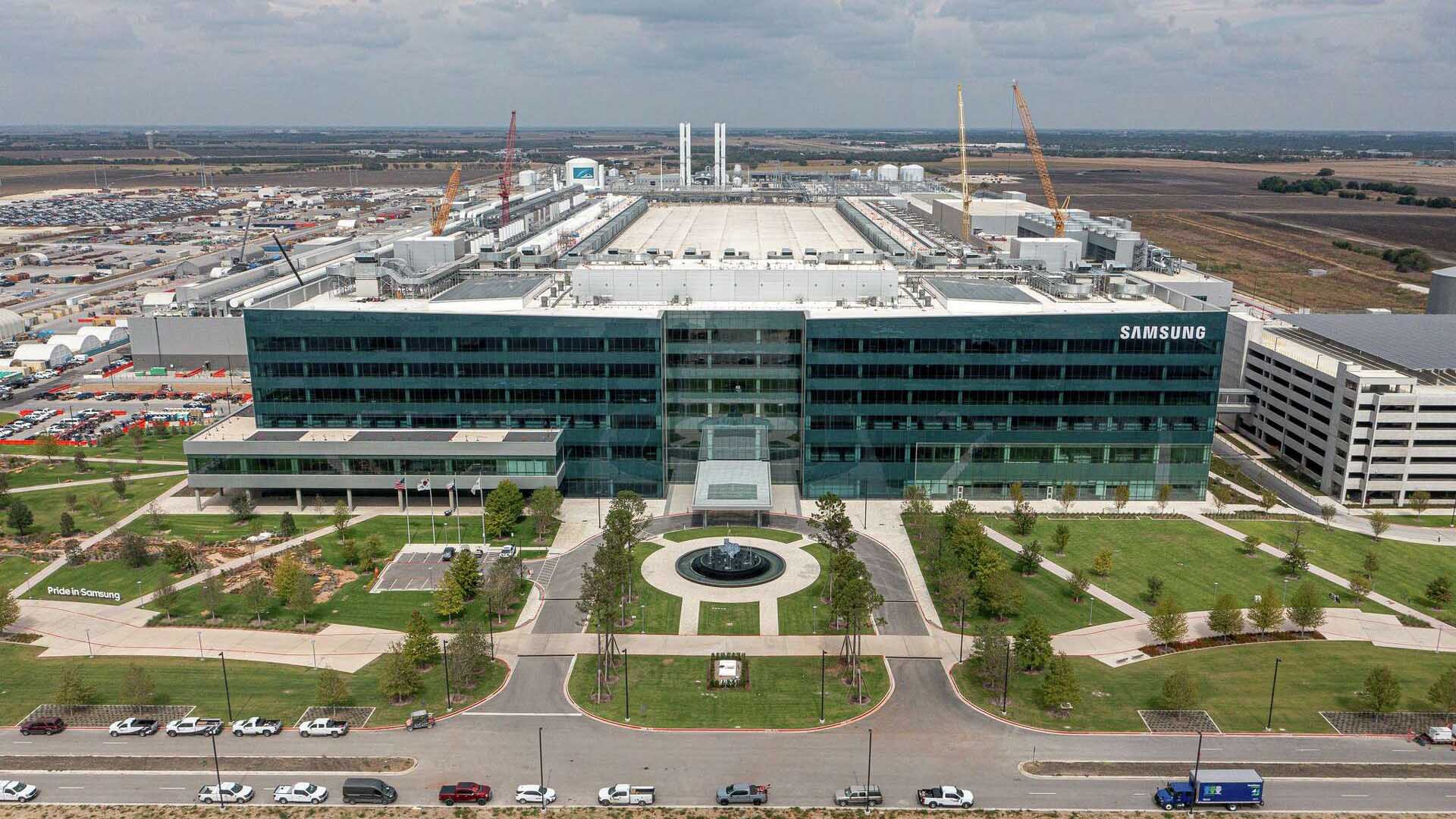
According to a report from Edaily, parts of the Taylor plant have now received a Temporary Certificate of Occupancy (TCO). This clearance allows specialized engineers to access the site and push work forward faster, helping accelerate equipment installation and operational readiness. Trial production had previously been expected to begin around March, and Samsung has reportedly staffed the effort heavily, with more than 7,000 employees involved in supporting the ramp.
A key piece of the 2nm puzzle is extreme ultraviolet (EUV) lithography, the advanced toolset required to manufacture chips at these tiny geometries. The report indicates EUV-related work is underway at the plant, with support teams assisting in deploying and configuring the equipment needed to run early production tests. Since 2nm GAA manufacturing depends on extremely precise tooling and process control, the trial phase will be crucial for validating performance, reliability, and repeatability.
If the trial run goes well, Samsung is expected to start operations at the Taylor plant this year, with full-scale manufacturing targeted for 2027. One detail causing some confusion is that the report also references 4nm production, even though industry expectations have pointed toward Taylor being upgraded for 2nm GAA. Either way, the broader direction is clear: Samsung wants Taylor to play a central role in its advanced-node strategy, not just as a legacy production site.
Samsung’s 2nm ambitions also come with growing customer interest in the U.S. The company is said to have multiple American customers lined up for its 2nm GAA node, with Tesla described as one of the most valuable. Beyond that, Samsung has reportedly secured orders from U.S.-based fabless chip companies and cloud service providers, strengthening its presence in the North American semiconductor ecosystem.
This U.S. expansion matters even more as demand for advanced chips continues to surge. With leading-edge capacity tight across the industry, customers are increasingly motivated to diversify manufacturing partners. If competitors are constrained at newer nodes, Samsung has an opening to win more business—especially from companies that need large volumes, predictable delivery timelines, and competitive pricing.
Still, the defining challenge for Samsung will be yield stability. Advanced nodes like 2nm are incredibly difficult to perfect, and yields directly influence both supply and cost. If Samsung can improve and stabilize 2nm GAA yields over time, it can lower wafer costs and become more aggressive on pricing. That combination—U.S.-based advanced manufacturing, expanding customer commitments, and improving yields—could help Samsung strengthen its position in the next phase of the semiconductor race.


