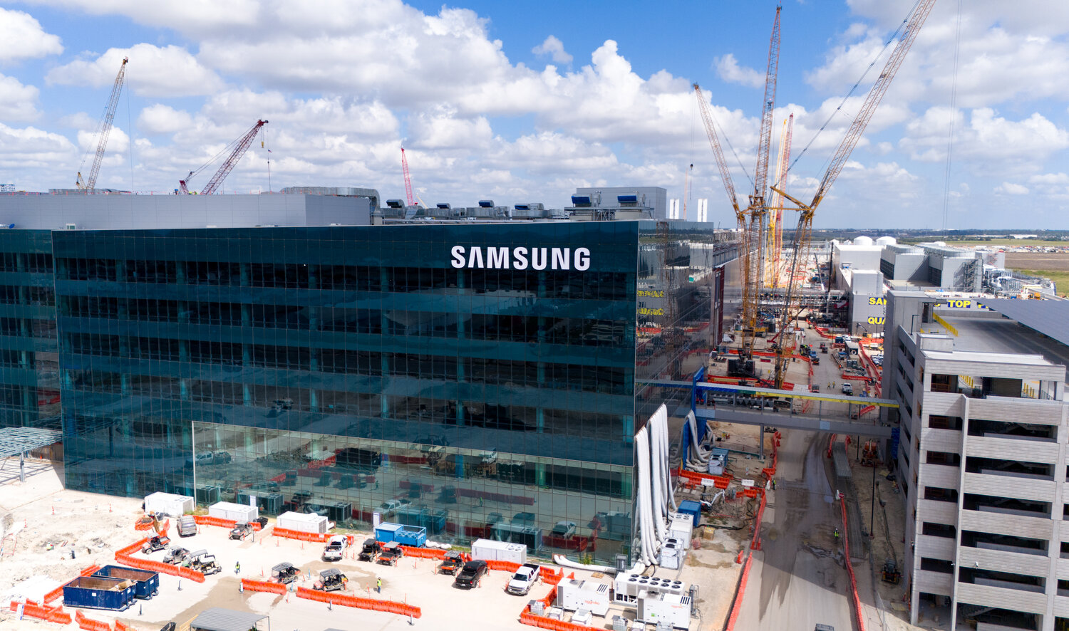
Samsung is moving closer to making the United States a major hub for cutting-edge chip manufacturing, with new reports saying the company will begin test operations of its extreme ultraviolet (EUV) lithography equipment at its Taylor, Texas facility in March. If the early trials go as planned, the Taylor site will become a key stepping stone toward Samsung’s bigger ambition: mass-producing next-generation 2nm Gate-All-Around (GAA) wafers on U.S. soil.
Taylor Plant 1 is expected to act as the testing ground for the critical stages of advanced semiconductor production, including installing EUV tools and running essential processes like etching and deposition. Full-scale manufacturing at the site is currently projected to start in the second half of 2026, positioning the Taylor facility as one of the most important U.S. manufacturing expansions Samsung has attempted in years.
While there’s no clear word yet on whether Samsung will manufacture mobile processors like the Exynos 2600 at Taylor, the report highlights a major customer already lined up: Tesla. Under a reported $16.5 billion agreement, Samsung is expected to produce Tesla’s autonomous driving chips, referred to as AI5 and AI6, at the Texas plant. That deal alone underscores why Taylor is being treated as far more than a symbolic investment—it’s meant to be a serious high-volume advanced node factory.
To keep the buildout on track, Samsung is reportedly preparing to apply for a Temporary Certificate of Occupancy (TCO), a required step that verifies the site meets fire safety and other local compliance standards. Construction progress is also being accelerated by a large on-site workforce, with around 7,000 workers involved. Once finished, the facility is expected to include a six-story building designed to support about 1,000 employees.
On sheer scale, Samsung’s Taylor footprint is enormous. The site is said to cover roughly 4.85 million square meters, making it larger in land area than Samsung’s major semiconductor facilities in Pyeongtaek and Hwaseong in South Korea. That size matters because Samsung isn’t thinking small—reports suggest the company has already secured enough space at Taylor to eventually build up to 10 plants, signaling long-term plans to turn the area into a multi-fab semiconductor campus.
Of course, the heart of this expansion is EUV. These machines are essential for producing leading-edge chips efficiently, especially at advanced nodes like 2nm. But they come with a jaw-dropping price tag—around 500 billion won (about $339 million) per EUV tool. For Samsung, buying and deploying EUV equipment at scale is a major financial commitment, yet it may be non-negotiable if the company wants to improve yield rates on its most advanced processes. The report points to current yields being around 50% on cutting-edge manufacturing, and boosting that figure is critical if Samsung’s foundry business is going to hit its profitability goals by 2027.
Those profitability targets come amid financial pressure. The report notes Samsung’s foundry operations have remained in the red, with an estimated $680 million deficit across the third and fourth quarters of 2025. That makes the Taylor ramp-up both a big bet and a potential turning point: get yields and volume right, and Samsung could secure major U.S.-based customers and strengthen its position in advanced contract chipmaking.
Interestingly, the Taylor site was once associated with 4nm production plans, but the direction appears to be shifting toward more advanced technology. With rivals cautious about bringing their most advanced manufacturing stateside, Samsung may see a window to differentiate itself in the U.S. market. One reported early target for the project is an initial mass production capacity of 50,000 wafers, suggesting Samsung is aiming for meaningful volume once the plant fully ramps.
In short, Samsung’s Taylor, Texas project is shaping up to be far more than a single fab. If the March EUV test operations succeed and the 2026 manufacturing start stays on schedule, the facility could become a cornerstone of U.S. advanced semiconductor manufacturing—supporting next-gen 2nm GAA production, high-profile customers like Tesla, and a longer-term roadmap that could eventually expand into a 10-plant mega-campus.


