Panel-Level Packaging and Glass Substrates Could Push Advanced Chip Packaging Beyond $8 Billion by 2030
The next major leap in semiconductor performance may not come only from smaller process nodes. It could come from how chips are packaged. As artificial intelligence and high-performance computing continue to demand more compute power, more memory bandwidth, and larger chip designs, the industry is moving toward advanced packaging technologies that can support bigger, faster, and more efficient processors.
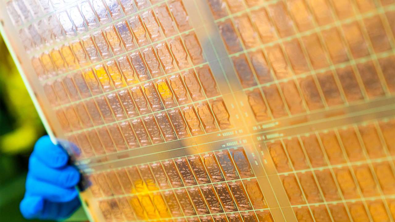
Fan-Out Panel-Level Packaging, often called FOPLP, and glass core substrates are emerging as two of the most important technologies for the next generation of AI and HPC chips. According to Counterpoint Research, the combined market for FOPLP and glass substrates is expected to surpass $8 billion by 2030, a major jump from around $650 million in 2024.
This rapid growth is being driven by the limits of traditional organic substrates and wafer-level packaging. As AI processors become larger and more complex, chipmakers need packaging methods that allow more dies, higher interconnect density, better thermal performance, and improved manufacturing efficiency. Panel-level packaging and glass substrates are designed to help solve these challenges.
Why AI and HPC chips need new packaging technologies
AI accelerators, GPUs, CPUs, and chiplet-based processors are becoming increasingly complex. Modern high-performance chips often combine compute dies, memory dies, interconnect layers, and other components into a single advanced package. This approach improves performance, but it also creates new manufacturing and engineering challenges.
Traditional organic substrates have served the semiconductor industry for decades, but they are facing limitations as package sizes increase. Warpage, signal integrity, thermal handling, and interconnect density become harder to manage at larger scales. Wafer-level packaging also has physical limitations because it is tied to the circular shape and size of silicon wafers.
FOPLP offers a larger packaging footprint by using rectangular panels instead of round wafers. This allows manufacturers to place more compute dies and DRAM dies on a single panel, improving production efficiency and potentially reducing costs. By 2030, panel-level packaging is expected to account for a significant share of market revenue, with estimates pointing to around 45.6%.
Glass substrates add another major advantage. Compared with organic materials, glass can offer better dimensional stability, lower warpage, higher interconnect density, and improved thermal characteristics. These traits are especially important for large AI processors and chiplet-based designs that require fast, dense connections between multiple components.
TSMC and Intel are pushing next-generation packaging forward
TSMC and Intel are among the leading companies accelerating the development of glass core substrates and panel-level packaging. These technologies are expected to play a key role in the future of advanced semiconductor manufacturing.
TSMC is advancing its Chip-on-Panel-on-Substrate approach, also known as CoPoS. The company is expected to begin with standard organic substrates before eventually transitioning to glass core substrates. Reports indicate that glass core substrates could reduce costs by around 30% while helping wafer utilization rates climb above 90%.
Intel has also been one of the most vocal supporters of glass substrate technology. The company introduced its glass substrate plans in 2023 and has continued to position the technology as a major step forward for next-generation processors. Intel and its partners are aiming to move toward commercialization of glass core substrates within the next few years.
Other major semiconductor and packaging players, including Samsung Electro-Mechanics, ASE, and PTI, are also expanding their work in glass substrates and panel-level packaging. As AI hardware demand grows, more companies are expected to invest heavily in these technologies.
Why glass substrates matter for future chip designs
Glass substrates could become a critical foundation for next-generation chip packaging because they address several problems found in traditional organic substrates.
They can support finer interconnects, allowing more electrical connections between chiplets and components. They also provide better dimensional stability, which helps reduce warpage when dealing with large packages. This is important because advanced AI processors are becoming physically larger and more difficult to manufacture reliably.
Yoshio Tamura, Vice President of Research at Counterpoint Research, noted that glass substrates are gaining industry attention as package complexity increases. Compared with organic materials, glass substrates can support higher interconnect density, stronger warpage control, and better stability, making them suitable for next-generation chiplet architectures and large AI processors.
These advantages could help chipmakers build larger AI accelerators with more memory, faster communication between dies, and better overall performance. For data centers, cloud computing, generative AI, and scientific computing, this could be a key enabler of future performance growth.
East Asia expected to dominate panel-level packaging capacity
By 2030, East Asia is expected to remain the main hub for FOPLP production capacity. Taiwan, China, and Japan are projected to account for approximately 84.8% of global panel-level packaging capacity by the end of the decade.
This reflects the region’s strong semiconductor supply chain, including foundries, packaging firms, materials suppliers, and equipment makers. Taiwan in particular remains a major center for advanced packaging development, while Japan continues to play a crucial role in materials and manufacturing technology.
The United States is also expected to strengthen its position in this field. Intel’s Rio Rancho facility is being developed as a key American hub for glass core substrates and panel-level packaging. This could help expand domestic advanced packaging capabilities as the semiconductor industry becomes more strategically important worldwide.
Challenges still need to be solved before mass adoption
Despite strong momentum, panel-level packaging and glass substrates still face several challenges before they can reach large-scale commercialization.
One major issue is the standardization of panel sizes. The industry needs common manufacturing standards to improve equipment compatibility, production efficiency, and supply chain stability.
Another challenge is consistency in Through-Glass Via, or TGV, interconnects. These vertical connections through glass are essential for enabling advanced electrical pathways, but producing them reliably at scale remains technically demanding.
Manufacturing stability is also critical. For these technologies to be adopted widely, chipmakers must be able to achieve high yields, predictable performance, and competitive costs. Without stable manufacturing processes, glass substrates and panel-level packaging may take longer to enter mainstream production.
The future of advanced packaging is becoming more important than ever
As chip scaling becomes harder and more expensive, advanced packaging is becoming one of the most important areas of innovation in the semiconductor industry. AI and HPC workloads require enormous processing power, and future performance gains will increasingly depend on how efficiently multiple dies, memory components, and interconnects can be integrated into a single package.
FOPLP and glass substrates offer a promising path forward. They can support larger packages, higher interconnect density, better thermal behavior, and improved production efficiency. With the market projected to exceed $8 billion by 2030, these technologies are no longer just experimental concepts. They are becoming central to the future of AI chips, high-performance computing processors, and next-generation semiconductor design.
If manufacturers can overcome standardization and production challenges, panel-level packaging and glass core substrates could become the backbone of the next era in advanced chip packaging.