Glass Core Substrate Prototypes With Co-Packaged Optics Offer a First Look at Future AI Chips
The next major shift in semiconductor packaging may have just taken a visible step forward. At the Optical Fiber Communication Conference 2026, early glass core substrate prototypes featuring co-packaged optics were shown, offering a preview of what high-performance AI and data center chips could look like near the end of the decade.
The prototypes were spotted by Dr. Ian Cutress of More Than Moore, who described them as mockups rather than production-ready chips. Even so, they provide an important glimpse into where advanced chip packaging is heading as the industry searches for new ways to handle the explosive growth of artificial intelligence workloads.
Why glass core substrates matter
Today’s advanced processors rely heavily on organic substrates, but demand from AI accelerators, high-bandwidth memory, and chiplet-based designs has put serious pressure on the supply chain. As AI hardware continues to scale, traditional substrate materials are facing limits in density, performance, and availability.
Glass core substrates are being explored as a major alternative because they can support much higher interconnect density, improved signal quality, and more advanced chiplet integration. Compared with organic substrates, glass can allow more chiplets to be placed in a single package while helping reduce signal loss and improving overall package efficiency.
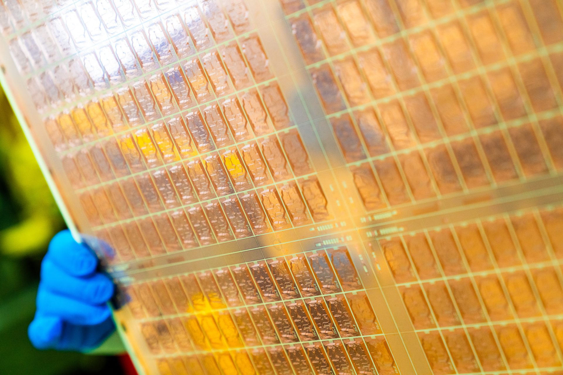
The prototypes shown at OFC 2026 included two different substrate designs: one based on ceramic material and another based on glass. The glass-based model stood out because of its transparent appearance, a direct result of the material itself. In contrast, traditional ceramic and organic substrates usually appear in darker tones such as purple-brown or green.
A closer look at the prototype design
The glass substrate mockup featured a complex multi-chip layout, including four compute chiplets, four DRAM chipsets, and eight smaller chipsets. However, the most eye-catching elements were the eight yellow chips placed around the edge of the glass substrate.
These yellow components represent co-packaged optical interfaces, a technology expected to play a major role in the future of AI and high-performance computing. Co-packaged optics bring optical communication closer to the processor package, reducing the need to move massive amounts of data through traditional copper connections.
Instead of relying only on electrical signals, optical transceivers convert data into light directly within or near the chip package. This can significantly improve bandwidth, reduce latency, and help lower power consumption in large AI data centers.
Co-packaged optics could reshape AI data centers
As AI models grow larger and more complex, moving data efficiently between chips, memory, and servers has become one of the biggest challenges in computing. Modern AI clusters require enormous bandwidth, and copper interconnects are increasingly struggling to keep up with the scale demanded by next-generation systems.
Silicon photonics and co-packaged optics are expected to help solve this issue by enabling much faster data movement across AI infrastructure. By placing optical interfaces close to compute silicon, future AI accelerators could achieve higher transfer speeds while reducing bottlenecks between chips.
Major chip companies are already racing to bring co-packaged optics into real-world hardware. The first commercial solutions are expected to arrive around 2027 to 2028, making the technology an important stepping stone toward the next wave of AI processors.
When will glass substrates arrive?
While the prototypes are promising, glass core substrates are not expected to become mainstream immediately. Intel has already confirmed work on glass substrate technology as a future replacement for organic packages. Its manufacturing partners have also suggested that commercial readiness could arrive within roughly three years.
Based on that timeline, the first meaningful rollout of glass core substrates could happen around 2029 to 2030. That timing aligns with expectations for future AI chips that will require denser packaging, more chiplets, more memory, and faster optical communication.
Why the industry is excited
The potential advantages of glass core substrates are significant. They may offer up to 10 times higher interconnect density compared with current organic substrates, making it possible to integrate more compute units, memory stacks, and specialized chiplets in a single package.
Glass substrates could also make it easier to integrate co-packaged optics, which is becoming increasingly important as AI systems demand faster and more efficient data movement. Another potential benefit is the use of rectangular panel-style manufacturing, which may improve yields compared with traditional round wafers.
If these benefits translate successfully into mass production, glass core substrates could become one of the most important packaging breakthroughs for future AI chips, HPC processors, and data center accelerators.
A glimpse of AI chips in 2029 and beyond
The glass core substrate prototypes shown at OFC 2026 are not final products, but they offer a realistic preview of what advanced processors may look like in the coming years. Future AI chips are likely to combine multiple compute chiplets, high-bandwidth memory, optical interfaces, and advanced packaging materials into highly integrated platforms.
With AI demand continuing to surge, the semiconductor industry needs more than faster transistors. It needs better ways to connect chips, memory, and systems together. Glass core substrates and co-packaged optics could become two of the key technologies that make the next generation of AI computing possible.
If development stays on track, the 2029 to 2030 period could mark the beginning of a new era in chip design, where glass-based packaging and optical data transfer help power the world’s most advanced AI data centers.