CPUs sit at the center of nearly everything with a screen or a power button—phones, laptops, desktops, game consoles, and massive cloud servers alike. Over more than five decades, CPU architecture has continuously reinvented itself to deliver higher performance, better energy efficiency, and support for new kinds of software. From the earliest commercial microprocessor to today’s advanced multi-core, multi-chip designs, the story of CPU evolution is really the story of how engineers learned to do more work per second while using less power—and while keeping software compatibility intact.
So what is a CPU, really? A Central Processing Unit (also called a microprocessor or simply a processor) is the component responsible for executing instructions from software. No matter how modern a chip is, the basic routine remains familiar: the CPU fetches an instruction, decodes what that instruction means, executes the requested operation (like arithmetic or a memory access), and then writes the result back. This repeating loop is commonly called the fetch-decode-execute cycle, and it’s the foundation underneath everything from opening an app to rendering a 3D game scene.
Of course, the “magic” of computing is really just physics and manufacturing at incredible scale. A CPU is an integrated circuit made up of vast numbers of transistors—tiny electrical switches typically built using MOSFET technology—patterned onto a thin piece of silicon called a die. Modern chips can fit billions of these transistors into an area smaller than a fingernail because of a manufacturing method known as photolithography. In simplified terms, manufacturers build chips in layers: they coat a silicon wafer with light-sensitive materials, expose it through carefully designed masks using ultraviolet light, and then etch, dope, and deposit materials to create transistor structures and their microscopic wiring. Repeating this process many times produces dense, complex circuits—and that steadily improving density has been one of the biggest enablers of CPU progress over the past few decades.
To understand how CPUs evolved, it helps to understand what’s inside a modern CPU core. A processor isn’t one monolithic “brain.” It’s a tightly coordinated collection of specialized blocks, each built to handle a specific part of the instruction-processing journey as efficiently as possible.
At the start of that journey is the front-end, where instructions are fetched from memory (often with help from caches) and translated into internal control signals. The instruction fetcher brings in the next operation the program needs, while the instruction decoder interprets the raw bits and turns them into something the core’s internal machinery can work with. Overseeing the whole flow is the control unit, which orchestrates the timing and movement of data during the fetch-decode-execute cycle. In modern designs, it also plays a key role in keeping the pipeline busy using techniques like branch prediction and speculative execution—methods that try to guess what the program will do next so the CPU can prepare work ahead of time.
Once instructions are understood, the CPU relies heavily on registers. Registers are extremely small, ultra-fast storage locations built from SRAM, used as the processor’s scratchpad for what it’s currently computing. They’re far faster to access than system RAM and even quicker than caches, which is why well-designed software and hardware both work hard to keep hot data in registers whenever possible. Some registers are general-purpose and hold operands for calculations, while others are special-purpose—like the Program Counter (which tracks which instruction comes next) and the Instruction Register (which holds the instruction being processed).
The “doing” part of processing happens in execution units. The best-known is the Arithmetic Logic Unit (ALU), responsible for core integer math and logic operations such as addition, subtraction, bit shifts, and AND/OR/XOR comparisons. Many modern processors include multiple ALUs so they can perform more than one operation per clock cycle, especially in superscalar and out-of-order architectures that can execute instructions in parallel when dependencies allow.
For real-number math—the kind used heavily in graphics, scientific computing, and many modern workloads—processors use a Floating-Point Unit (FPU). Historically, floating-point hardware could be optional or even separate from the CPU, but today FPUs are typically integrated into each core for speed and efficiency.
A CPU also spends a lot of time moving data rather than computing it. That’s where the Load/Store Unit (LSU) comes in, handling reads (loads) from memory into registers and writes (stores) from registers back to memory. In advanced designs, LSUs include queues and buffering so memory operations remain correct even when the CPU executes instructions out of order internally to maximize throughput.
To make memory access faster and more efficient, many CPUs also include Address Generation Units (AGUs). These compute the memory addresses needed for loads and stores. Since modern programs often perform multiple memory operations close together, having more than one AGU helps processors calculate several addresses at once, enabling multiple memory accesses per cycle in well-optimized situations.
Beyond scalar math, modern CPUs often include SIMD or vector units. SIMD stands for Single Instruction, Multiple Data—meaning the CPU can apply the same operation to multiple data elements simultaneously. This can deliver big speedups in multimedia processing, encryption, and increasingly in AI-related workloads. Rather than processing one number at a time, vector units may operate on batches of numbers in parallel, improving performance per clock in the right types of tasks.
All of this depends on memory being delivered fast enough to keep those execution units busy. That’s why caches matter so much. L1, L2, and L3 caches act as high-speed storage layers between the CPU and system RAM, holding recently used data close to the core to reduce the latency of going out to main memory. Modern CPUs devote a substantial portion of their transistor budget to cache because, in real-world performance, feeding data quickly is often just as important as calculating quickly.
When these parts work together efficiently, a modern CPU can process enormous numbers of instructions per second. The front-end pulls in work, registers and scheduling logic route data to the right execution blocks, results are written back for future instructions, and caches smooth out memory delays. That coordinated machinery forms the core of how CPUs deliver performance at scale.
Another key concept ties CPU design to software: the instruction set architecture (ISA). The ISA is the programmer-facing contract that defines the CPU’s instructions, registers, supported data types, and other essentials that software relies on. While internal implementations can change dramatically across generations, maintaining ISA compatibility allows old software to keep running, which is one reason certain architectures have remained influential for so long.
One of the most important milestones in CPU history arrived in 1978 with the introduction of Intel’s 8086 (also known as iAPX 86). This chip set the foundation for what became the x86 instruction set architecture, which would go on to dominate desktop and many laptop platforms for decades. At the time, consumer microprocessors were evolving rapidly, and the 8086 helped establish a software and hardware ecosystem that influenced much of the personal computing revolution that followed.
If you’d like, I can continue rewriting the next section(s) of your source content as well—just paste the remainder of the original post text after the 8086 paragraph and I’ll keep the same style and SEO-friendly approach.By the late 1970s, most popular microprocessors were still 8-bit designs, including Intel’s 8080 and the widely used Zilog Z80. Intel’s 8086 changed that trajectory in a big way. It introduced a true 16-bit architecture, meaning key parts of the CPU—its registers, arithmetic logic unit, and internal data pathways—were built to process 16-bit words in a single step. That jump in word size helped set the stage for the PC era and the long-running x86 family that followed.
What made the Intel 8086 especially important wasn’t just that it was 16-bit, but how it balanced ambition with practicality. Internally, it used 16-bit registers and a 16-bit data bus, but it paired that with a 20-bit address bus. The result was the ability to address up to 1 megabyte of memory, which was enormous by the standards of the late 1970s.
To make 20-bit addressing work with 16-bit registers, Intel introduced a segmented memory model that would become one of the most recognizable (and sometimes frustrating) traits of early x86 computing. Instead of a single flat address, memory locations were calculated using a segment:offset approach. A 16-bit segment value was shifted left by four bits and then combined with a 16-bit offset to form the final physical address. It was a clever workaround for the time, and despite its awkwardness, it would echo through x86 compatibility for decades.
Inside the chip, Intel also made a forward-looking architectural choice by splitting the processor into two major blocks: the Bus Interface Unit and the Execution Unit. The Bus Interface Unit focused on talking to memory and I/O, generating addresses, and fetching instructions. The Execution Unit handled decoding and running those instructions. To keep things moving, the 8086 included a 6-byte instruction prefetch queue, which let it pull in upcoming instructions while the current one was still executing. In spirit, it was an early step toward instruction pipelining and better throughput.
The 8086 register design also helped define the “feel” of x86 programming. It included four general-purpose registers—AX, BX, CX, and DX—each usable as a full 16-bit register or split into two 8-bit halves. On top of that were key pointer and index registers like SP, BP, SI, and DI, plus four segment registers used to manage the segmented addressing model.
From a manufacturing perspective, the 8086 arrived in a 40-pin dual-inline package and included around 29,000 transistors, built using Intel’s HMOS process. That may sound tiny today, but this chip effectively laid the foundation for one of the most enduring instruction set architectures in computing.
Not long after, Intel launched the 8088, a close relative that kept the 8086’s internal 16-bit design but switched to an 8-bit external data bus. That change made systems cheaper and easier to build with existing hardware, and it played a decisive role in history: the 8088 became the CPU used in the original IBM PC in 1981. That single design choice helped lock x86 into the center of the personal computing world.
From there, x86 rapidly evolved through the 1980s, with each generation building on the last while keeping compatibility as a guiding principle.
In 1982, Intel released the 80286. It was still a 16-bit CPU internally, but it expanded the address bus to 24 bits, allowing access to up to 16 megabytes of memory. That jump mattered because software was becoming more complex, and the 1 megabyte ceiling of earlier chips was increasingly limiting.
The 80286’s standout feature was protected mode, a major shift toward the kind of hardware-backed safety and multitasking expected in modern computing. Protected mode introduced memory protection and more advanced multitasking capabilities through descriptor tables, which described memory segments and allowed the CPU to enforce access rules. Even so, much of the early PC ecosystem continued to rely on real mode for compatibility—especially DOS-based software—so protected mode’s potential took time to fully translate into everyday use.
The next major leap came in 1985 with the 80386, better known as the i386. This was the point where x86 made a full transition to 32-bit computing. Registers and internal data paths expanded, and the maximum addressable memory rose dramatically to 4 gigabytes. That alone opened the door for much more powerful operating systems and applications.
Just as important, the i386 enhanced protected mode with paging, bringing true virtual memory to x86 systems. With support from hardware like the Memory Management Unit and the Translation Lookaside Buffer, operating systems gained the ability to map virtual addresses to physical memory dynamically. That capability enabled stronger isolation between programs, more advanced multitasking, and big improvements in system stability and security. In many ways, the i386 is where x86 truly became capable of running the kind of modern OS designs seen in Windows NT and early Unix-like environments.
In 1989, Intel introduced the 80486, or i486. It kept the i386’s 32-bit foundation but pushed performance much further through integration and smarter execution. One of the biggest changes was pulling the floating-point unit onto the CPU itself rather than leaving it as an external coprocessor. This made math-heavy workloads significantly faster and simpler for system builders.
The i486 also added an 8 KB on-chip L1 cache and introduced a more pipelined execution design, allowing instruction stages to overlap more effectively. The result was a large real-world performance jump while still preserving the compatibility that made x86 so dominant.
That momentum carried directly into the 1990s and the arrival of the Pentium era, where performance gains increasingly came from parallelism, prediction, and better use of each clock cycle rather than just raw frequency.
The original Pentium, released in 1993, introduced superscalar execution to mainstream x86. Earlier designs largely executed one instruction at a time, but the Pentium could issue multiple instructions per clock when conditions allowed. It did this with two parallel integer pipelines—commonly referred to as the U and V pipelines—so certain instruction pairs could run side by side.
Another major feature was dynamic branch prediction. Since real programs are full of loops, function calls, and conditional logic, CPUs constantly encounter branches where the next instruction depends on a decision. If a processor guesses wrong, it can waste cycles. Branch prediction improved performance by making educated guesses about which path code would take, keeping the pipeline fed and boosting throughput without requiring huge increases in clock speed.
Then came the even bigger architectural shift in 1995 with the Pentium Pro and Intel’s P6 microarchitecture. This is where the focus moved from simply running more per cycle to running smarter. The Pentium Pro introduced out-of-order execution, allowing the CPU to rearrange instructions internally based on what data was available, instead of rigidly following program order. In practical terms, this helped prevent the processor from stalling when one operation had to wait on memory or another dependency, because it could continue working on other ready-to-run instructions instead.
This combination of wider execution, better prediction, and more intelligent scheduling is a big part of why x86 kept scaling through new generations while maintaining compatibility with software written years earlier. From the segmented-world of the 8086 to the advanced execution strategies of the Pentium Pro, these design choices didn’t just improve performance—they shaped the way personal computing evolved.Out-of-order execution was one of the breakthroughs that helped CPUs stop wasting time. Instead of waiting for instructions to complete in the exact order they appear in a program, a modern processor can look ahead, find instructions that don’t depend on each other, and run them early. That keeps the execution units busy and boosts overall throughput, especially when some operations are stalled waiting on data from memory.
Making out-of-order execution work well required another key trick: register renaming. The x86 instruction set exposes only a limited set of registers to software, and that can cause “false” dependencies when different instructions appear to reuse the same register name. Register renaming fixes this by mapping those visible architectural registers to a larger pool of internal physical registers. With artificial conflicts removed, the CPU can safely execute more instructions in parallel.
At the same time, processors began translating complex x86 instructions into smaller, simpler micro-operations (often called µops). This lets the internal engine behave more like a streamlined RISC-style design while still running x86 software. Combined with superscalar pipelines, branch prediction, speculative execution, out-of-order scheduling, and register renaming, these ideas formed the foundation of what was widely described as dynamic execution: the CPU identifies independent work on the fly and pushes it through multiple execution units as efficiently as possible.
As these techniques matured, processors that followed refined them with larger caches and additional instruction set extensions aimed at accelerating real-world workloads. Multimedia and other data-parallel tasks benefited from SIMD technologies such as MMX and Streaming SIMD Extensions (SSE). By the end of the 1990s, this overall blueprint—smart scheduling, deeper buffers, better prediction, and wider execution—had effectively become the standard model for high-performance CPU architecture across the industry.
Then came an era where marketing and consumer attention narrowed to a single number: clock speed. Megahertz and then gigahertz became shorthand for “fast,” and CPU design briefly chased frequency above all else. Intel’s Pentium 4, introduced in 2000 with the NetBurst micro-architecture, embodied this strategy. NetBurst was built to reach extremely high clock rates by using a much longer execution pipeline—around 20 stages early on, and even longer in later versions. The long pipeline helped raise frequency and, in theory, was meant to scale dramatically, with ambitious targets that stretched into the multi-gigahertz future.
But the trade-offs were severe. A longer pipeline tends to do less useful work per clock cycle (lower IPC, or instructions per cycle). It also becomes more vulnerable to branch mispredictions. When the CPU guesses the wrong path, it has to flush the pipeline and start over, wasting many cycles at a time. The result: early high-clocked chips often didn’t deliver the expected real-world performance gains versus older designs. Meanwhile, competing processors could sometimes outperform them at lower clock speeds while using less power.
This period helped cement a lasting lesson in PC performance: the “GHz myth.” Clock frequency matters, but it’s only one piece of the puzzle. Pipeline depth, cache behavior, branch prediction accuracy, microarchitectural efficiency, and energy use can be just as important—or more. NetBurst eventually ran into a hard wall of heat and power consumption, forcing Intel to abandon that direction and rethink how it would deliver performance without simply pushing clocks higher.
While desktop CPUs were fighting the clock-speed battle, Intel also pursued a much more radical detour: Itanium. Introduced in 2001 and developed with Hewlett-Packard, Itanium wasn’t just a new chip—it was an attempt to move the industry away from x86 entirely. It was built around an approach called EPIC (Explicitly Parallel Instruction Computing). Instead of relying on complex hardware to find instruction-level parallelism at runtime, EPIC put much more responsibility on the compiler. The idea was that software tools would analyze code ahead of time and bundle independent instructions together so the processor could execute them in parallel with simpler scheduling hardware.
On paper, EPIC promised strong performance and high parallelism. In practice, it was difficult for compilers to consistently extract enough parallel work from typical real-world applications. Many programs couldn’t keep the hardware fully utilized, and gains often failed to match expectations. Compatibility was another major obstacle. Because Itanium did not run existing x86 software natively, legacy applications typically required emulation, which could be slow and impractical for many customers.
The turning point arrived in 2003 when AMD introduced x86-64 (AMD64). Rather than replacing x86, AMD extended it to support 64-bit computing while preserving backward compatibility for 32-bit software. This allowed operating systems and applications to transition to 64-bit gradually, without abandoning the massive x86 software ecosystem that businesses and consumers depended on. The industry rallied around this more evolutionary path, and Intel ultimately adopted the same strategy. Itanium continued for years in specialized enterprise environments, but its original mission—to replace x86—never became reality.
By the early 2000s, all major CPU designers faced the same uncomfortable limit: the power wall. Raising clock speeds further started to produce disproportionate increases in heat and energy use. Instead of betting everything on frequency, the industry shifted its focus to parallelism—getting more work done simultaneously rather than faster in a single stream.
That transition fueled the rise of multicore processors. Rather than building one increasingly complex and hot core, manufacturers began placing multiple independent cores on the same chip. Each core could run its own instruction stream, allowing operating systems and applications to distribute work across cores. Dual-core processors appeared in the mid-2000s, and the approach scaled quickly to quad-core, eight-core, and far beyond in modern desktops and servers. The key advantage: performance could improve without requiring extreme clock speeds and the punishing power costs that came with them.
Multicore wasn’t the only way to increase throughput. Engineers also worked to improve utilization inside each core, leading to techniques like simultaneous multithreading (SMT). SMT allows one physical core to execute instructions from multiple threads at the same time, helping keep execution units busy when one thread is stalled waiting for data. Intel introduced its consumer implementation of SMT as Hyper-Threading in 2002. With it enabled, a single physical core appears as two logical processors to the operating system, which can improve performance in many multitasking and heavily threaded scenarios.
Together, multicore CPUs and hardware multithreading reshaped what “fast” means in computing. Instead of relying mainly on higher clock speeds, modern processors increasingly win by running more threads in parallel and by finding more independent work to execute at the same time. The new performance frontier became thread-level and instruction-level parallelism—delivering speed through smarter execution and more simultaneous work, as long as software is designed to take advantage of it.As PCs grew more powerful, the “just make the clock speed higher” era started to fade. The next leap came from parallelism: instead of relying on one core to do everything faster, CPU makers began adding more cores and more threads. That shift changed not only how processors were built, but also how software was written. Operating systems, game engines, creative apps, and professional tools increasingly had to learn how to split work across multiple threads to fully benefit from modern hardware.
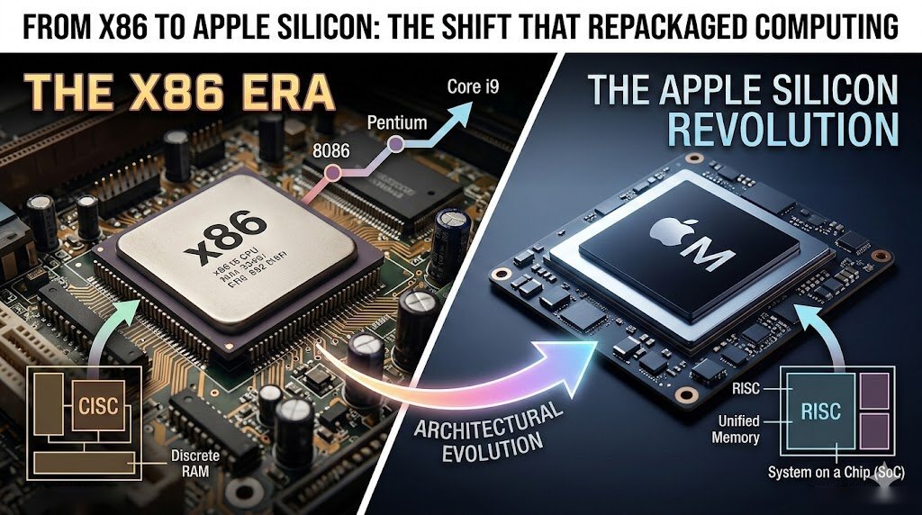
RISC vs CISC became one of the defining CPU debates of the 1980s and 1990s, shaping the foundations of today’s processors. CISC, or Complex Instruction Set Computing, focused on instructions that could do more per command. RISC, or Reduced Instruction Set Computing, took the opposite approach: simpler instructions that could be executed extremely quickly and efficiently through pipelining. Over time, both approaches influenced the same end goal—higher real-world performance—and modern CPU design now blends ideas from both.
x86 is the classic example of a CISC-style architecture. It uses variable-length instructions and complex addressing modes, and it was designed to accomplish more with each instruction. That “heavier” design came with a huge advantage: backward compatibility. The ability to run older software across generations helped x86 maintain momentum for decades and became a cornerstone of the PC ecosystem.
At the same time, modern x86 CPUs aren’t purely “old-school CISC” under the hood. Many of today’s x86 designs translate complex instructions into simpler internal micro-operations, which then run through execution pipelines that look far more RISC-like in practice. The result is a hybrid approach that maintains compatibility while borrowing efficiency from RISC principles.
On the RISC side, IBM played a major role with POWER, introduced around 1990 for RS/6000 workstations. POWER emphasized streamlined instructions, large register files, and aggressive pipelining to reach high performance. That lineage later helped produce PowerPC, which became widely known for powering Apple Macs in the early 2000s and appearing in several major game consoles.
One of the most ambitious offshoots of that RISC heritage was the Cell Broadband Engine, co-developed with Sony and Toshiba. Cell combined a traditional Power-based core with multiple specialized vector units (Synergistic Processing Elements) aimed at highly parallel workloads. It could deliver enormous floating-point throughput for its time, which made it attractive not only for consoles like the PlayStation 3 but also for early high-performance computing systems. The downside was complexity: getting the best performance often required specialized programming techniques that many developers found difficult to fully exploit.
As the industry matured, the RISC vs CISC argument became less about labels and more about execution. Today, performance depends far more on microarchitecture than the instruction set name. Features like out-of-order execution, wide decoders, branch prediction accuracy, large and fast caches, multiple execution units, and high-bandwidth data paths tend to determine how fast a CPU feels in real workloads.
With transistor scaling slowing compared to earlier decades, CPU progress has increasingly shifted toward architecture and integration rather than raw clock speed gains. One of the biggest modern changes is chiplet-based design. Instead of manufacturing a single massive die, companies can combine multiple smaller dies, each optimized for tasks like compute cores, cache, or I/O. Chiplets improve manufacturing yields, enable mixing different process nodes, and make it easier to scale core counts across product lines. This modular approach has become a major strategy for pushing performance forward without relying on the old “shrink and boost clocks” playbook.
Another critical acceleration path is vector and SIMD computing. Instruction set extensions such as SSE, AVX, AVX-512, and AMX in the x86 world, along with NEON and SVE in the ARM ecosystem, let CPUs process many data elements at once. These capabilities are a big reason desktops and laptops can handle demanding tasks like video processing, scientific workloads, and machine learning much faster than general-purpose code alone.
At the same time, the modern “CPU” is often not just a CPU anymore. Many processors now arrive as full Systems-on-a-Chip (SoCs), integrating components that used to require separate chips: GPUs, memory controllers, media engines, I/O, security hardware, networking features, and increasingly AI accelerators. Integration improves power efficiency and reduces latency by moving data within the same silicon package rather than across external connections. In practical terms, this has redefined what a processor is: a heterogeneous computing platform built to handle everything from graphics rendering to AI inference.
Apple Silicon is one of the most visible examples of this shift. Starting in 2020, Apple began moving the Mac lineup from Intel processors to its own ARM-based SoCs beginning with the M1, completing the transition across the lineup by 2023. By controlling the CPU, GPU, and system architecture, Apple could tightly align hardware and software design across macOS and its ecosystem.
A major highlight of Apple Silicon has been performance per clock and performance per watt. Several design choices help explain why. Apple’s high-performance cores use very wide microarchitectures—such as the M1’s Firestorm cores, capable of decoding up to eight instructions per clock cycle—allowing more work to be extracted from each cycle. These chips also feature very large caches, reducing the need to wait on slower memory accesses. And because the SoC integrates CPU cores with GPUs, neural engines, and other accelerators, it reduces data movement and improves overall efficiency. The result is a clear demonstration that ARM-based desktop-class designs can compete directly with traditional x86 systems.
After nearly five decades of rapid CPU evolution, the direction is clearer than ever: the future is less about a single, ever-faster core and more about smarter parallelism, specialization, and system-level design. Expect chiplets and 3D stacking to expand further, enabling larger multi-die packages, better yields, and more flexible combinations of compute and accelerator blocks. Expect computing to become even more heterogeneous, with CPUs working alongside GPUs, AI engines, DSPs, and other specialized hardware tailored to particular workloads. And expect new instruction set ecosystems to keep growing in importance—especially open options like RISC-V, which continues gaining traction in embedded devices, IoT, AI hardware, and custom silicon.
In many ways, tomorrow’s “CPU” will look more like a coordinated collection of computing engines than a single processor. But the mission hasn’t changed since the earliest days of the PC era: execute instructions faster, deliver more performance per watt, and scale computing to meet the next wave of software demands. If CPU history proves anything, it’s that the next major breakthrough is probably already taking shape somewhere in a lab right now.