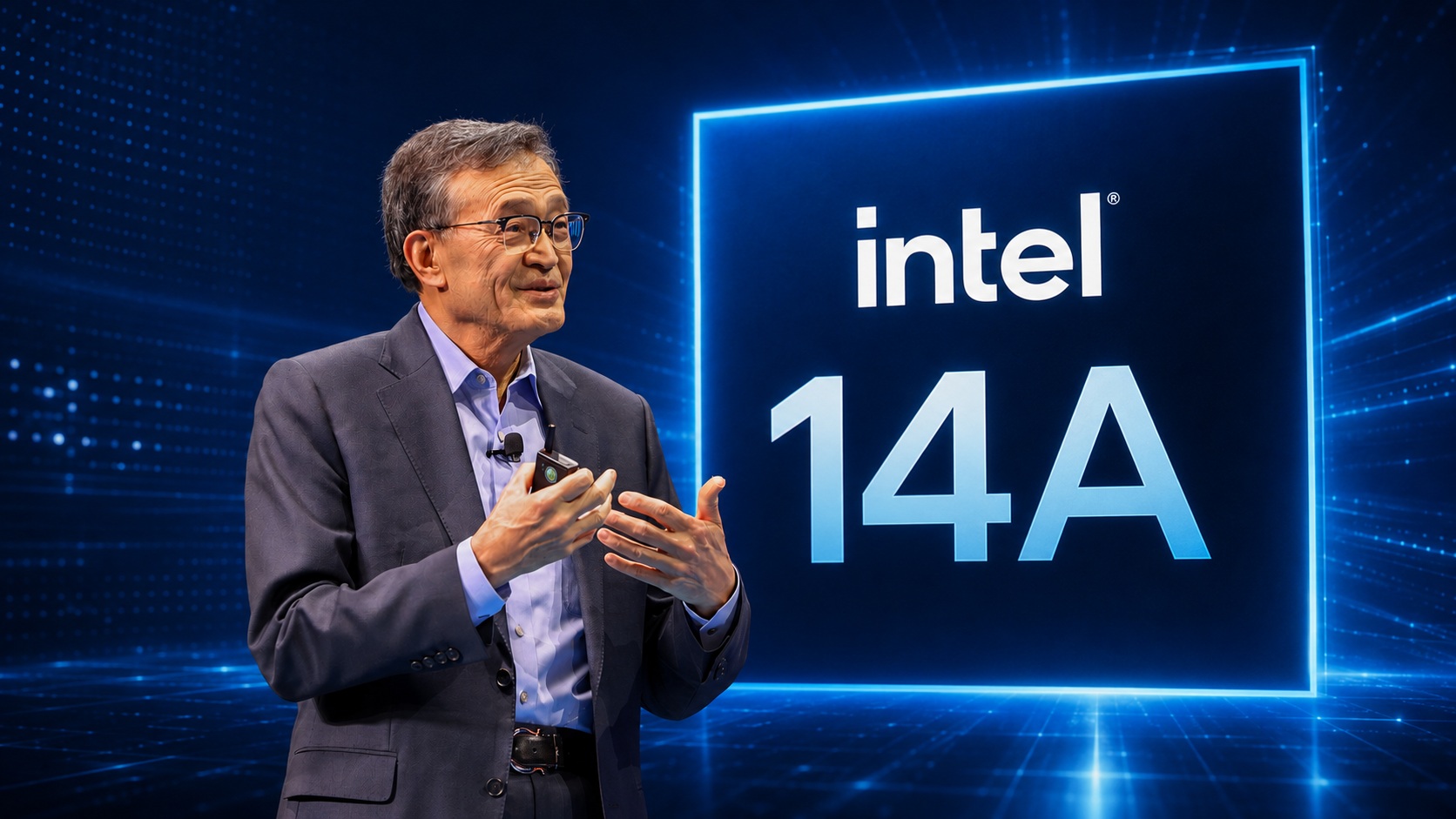
Intel Says 14A Chip Process Is Improving at Its Fastest Pace Since the 22nm Era
Intel’s next major chipmaking technology, known as 14A, appears to be gaining momentum as the company pushes deeper into advanced semiconductor manufacturing and foundry services. According to Intel Chief Financial Officer David Zinsner, progress on the 14A process is moving faster than any Intel manufacturing node since the company’s landmark 22-nanometer technology introduced in 2012.
Speaking at Deutsche Bank’s 2026 Technology Conference, Zinsner discussed the pace of improvement in Intel’s 14A process, particularly around defect density. In semiconductor manufacturing, defect density refers to the number of flaws or contaminations found within a given area of a wafer. Lower defect density is critical because it generally leads to better yields, improved chip performance, and stronger production economics.
Intel’s 14A node is one of the most important technologies in the company’s long-term roadmap. It is expected to play a central role in Intel’s effort to compete more aggressively in the global contract chip manufacturing market, where Taiwan Semiconductor Manufacturing Company remains the dominant player.
The company has already confirmed that 14A is expected to enter risk production in 2027, followed by volume production in 2028. Risk production is an early manufacturing stage used to test the readiness of a process before mass production begins. Intel had previously suggested a later timeline, so the updated schedule reflects a more ambitious push to bring the technology to market.
Zinsner’s latest remarks build on comments he made in 2025, when he said Intel’s 14A process looked stronger than 18A did at the same stage of maturity, particularly in terms of performance and yield. Now, he says the defect-density improvement curve for 14A is tracking similarly to Intel’s 22nm node, a historically significant technology for the company.
The comparison matters because Intel’s 22nm process was a major milestone in the semiconductor industry. It was the first Intel node to introduce FinFET transistor technology, a design that helped improve power efficiency and performance while enabling continued transistor scaling.
Another important detail from Zinsner’s comments is that Intel has already started designing initial products for the 14A process. This suggests the technology is advancing beyond early development and could be attracting interest from internal teams or external foundry customers.
Customer demand is a key factor for the future of 14A. Intel’s foundry strategy depends not only on building advanced manufacturing technologies but also on convincing major chip designers to use them. Company executives have previously acknowledged that if customer interest is not strong enough, the economics of future manufacturing nodes could become more difficult.
Intel is also working on a second-generation version of the technology called 14A2. This follow-up process is expected to improve power delivery by using both the front and back sides of the chip. Backside power delivery is becoming increasingly important as advanced chip designs shrink and traditional wiring faces greater electrical challenges, including voltage drops and signal limitations.
As chips become denser and more complex, improving power delivery is essential for boosting performance and efficiency. Technologies like 14A2 could help Intel address these challenges while making its foundry offerings more competitive for high-performance computing, artificial intelligence, and next-generation processor designs.
For Intel, the stakes are high. The company’s ability to execute on 14A and future nodes will be closely watched by investors, chip designers, and the broader semiconductor industry. If Intel can deliver strong yields, competitive performance, and reliable production timelines, 14A could become a major turning point in its effort to regain leadership in advanced chip manufacturing.