Elon Musk Says IBM’s 0.7-Nanometer Chip Naming Is Misleading
Elon Musk has weighed in on IBM’s latest semiconductor announcement, arguing that the way advanced chipmaking technologies are named has become confusing and potentially misleading.
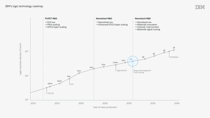
IBM recently revealed what it describes as a 0.7-nanometer, or 7-angstrom, chip manufacturing technology, calling it one of the most advanced semiconductor process developments in the world. The company says the breakthrough builds on nanosheet transistor technology and uses a technique called nanostacking, which allows transistors to be stacked vertically to improve chip density and performance.
According to IBM, wafer bonding is also an important part of the new process. This technique helps combine different layers of silicon, enabling more compact and powerful chip designs as the semiconductor industry pushes beyond traditional scaling methods.
However, Musk believes the “0.7-nanometer” label does not accurately describe the physical size of the smallest features on the chip. Responding to criticism on X, Musk agreed that modern process-node naming no longer reflects real transistor dimensions in the way it once did.
He suggested that chip manufacturing nodes should instead be named based on the number of atoms across the smallest feature size. In Musk’s view, that would provide a clearer and more scientifically accurate way to describe semiconductor technology.
The debate highlights a growing issue in the chip industry. Years ago, process-node names such as 90nm, 45nm, or 22nm were more closely tied to actual physical measurements inside a chip. But as chip designs became more complex, those numbers evolved into marketing and generation labels rather than direct measurements of transistor gate length or metal pitch.
IBM acknowledged this shift in its own explanation of the 7-angstrom process. The company stated that, like other recent advances in transistor technology, the 7-angstrom name refers to a new generation of chips made with a specific manufacturing process. It does not directly represent the width of contacted metal wires, as it did in much older chip generations.
This is not a new controversy. Semiconductor companies have been adjusting naming conventions for years as competition in advanced chip manufacturing has intensified. Intel, for example, revised its process roadmap in 2021, renaming its 10-nanometer technology as Intel 7 and its 7-nanometer technology as Intel 4. The move was part of a broader effort to make its process names more comparable with rivals in the global foundry market.
The competition is especially fierce because advanced chip manufacturing has become central to artificial intelligence, consumer electronics, data centers, electric vehicles, and high-performance computing. Companies such as TSMC have become critical manufacturing partners for major technology firms, producing chips for AMD, NVIDIA, Apple, and others.
Musk’s comments also connect to his broader interest in computing infrastructure. He has been involved in efforts to rapidly expand AI computing capacity, including large-scale projects designed to deliver enormous amounts of processing power. For companies racing to build more capable AI systems, chip density, energy efficiency, and manufacturing scale are increasingly important.
IBM’s 0.7-nanometer announcement is still significant because it points toward the future of semiconductor design, where stacking, bonding, and new transistor architectures may become just as important as shrinking traditional features. But Musk’s criticism reflects a larger concern: if chip names no longer describe actual physical measurements, consumers, investors, and even some industry observers may misunderstand what the numbers really mean.
As chipmakers move into the angstrom era, the industry may face growing pressure to create clearer naming standards. Whether companies adopt Musk’s atom-based suggestion remains to be seen, but the conversation shows that semiconductor branding is no longer just a technical detail. It has become part of the battle for trust, credibility, and leadership in the race to build the next generation of computing technology.