IBM Unveils 0.7-Nanometer Chip Technology With Up to 100 Billion Transistors
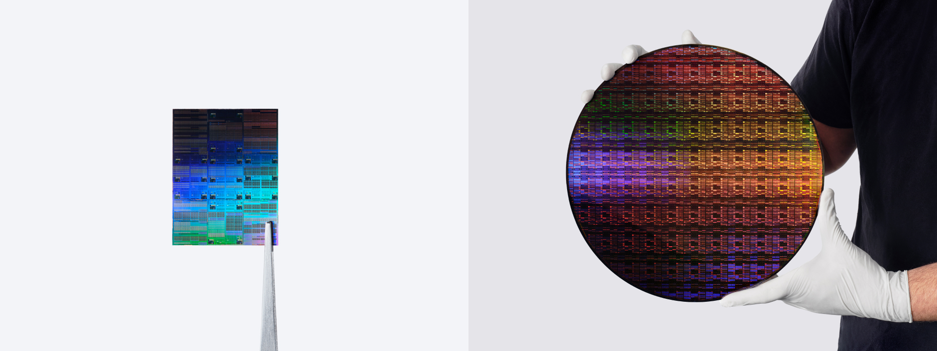
IBM has announced a major breakthrough in semiconductor technology with the introduction of its 0.7-nanometer chip process, making it one of the first companies to reveal a chip manufacturing technology below the 1-nanometer node. The company says this next-generation process could allow chips to hold up to 100 billion transistors in an area roughly the size of a fingernail.
At the center of the announcement is IBM’s new nanostack technology, an advanced approach designed to push transistor density and chip efficiency far beyond current limits. The development marks another step in the race to build smaller, faster, and more power-efficient processors for artificial intelligence, high-performance computing, mobile devices, and future data centers.
IBM says its 0.7-nanometer process delivers nearly double the density of its 2-nanometer technology, which was introduced in 2021. At that time, IBM’s 2-nanometer chip design used nanosheet transistors and promised up to 45% better performance or up to 75% lower power consumption compared with leading 7-nanometer technologies available then.
The new 0.7-nanometer technology builds on that foundation but introduces a more advanced structure. IBM describes nanostack as an evolution of nanosheet chip design. Instead of relying only on horizontal transistor layouts, nanostack technology vertically stacks and staggers transistors, creating a 3D structure that allows more components to fit into the same chip area.
This 3D transistor integration could be critical for the future of semiconductor manufacturing. As traditional chip scaling becomes increasingly difficult, companies are exploring new ways to increase transistor density without simply shrinking every feature in the same old manner. IBM’s nanostack design aims to solve that challenge by building upward as well as across the chip surface.
According to IBM, its nanostack architecture has been experimentally validated using ultra-thin dielectric bonding in CMOS integration. This process requires extremely precise alignment between transistor layers, making manufacturing accuracy one of the most important parts of the technology.
The performance claims are significant. IBM says 0.7-nanometer chips could offer up to 70% higher power efficiency or up to 50% better performance compared with its 2-nanometer technology. If achieved in commercial production, those gains could have a major impact across the computing industry.
Artificial intelligence workloads may be among the biggest beneficiaries. IBM estimates that an AI chip using the 0.7-nanometer process, also referred to as 7A technology, could increase performance from around 4,500 trillion operations per second to 9,000 trillion operations per second. That level of improvement could dramatically reduce AI training times, potentially cutting a process that takes three months down to just a few weeks.
The company also shared details about how it created the nanostack structure. IBM developed a new wafer bonding technique that joins two wafers to form a multilayered structure. This method enables the creation of 3D transistors that could serve as the foundation for future generations of advanced computer chips.
Nanosheet transistor technology has already become an important direction for the semiconductor industry, especially as older FinFET designs approach their scaling limits. By moving from nanosheets to stacked 3D transistor structures, IBM is signaling that the next era of chip innovation may depend not only on smaller process nodes but also on smarter chip architecture.
While commercial products based on 0.7-nanometer technology may still be years away, IBM’s announcement highlights the rapid progress being made in semiconductor research. Smaller and more efficient chips are essential for powering future AI systems, cloud infrastructure, consumer electronics, and scientific computing.
If IBM’s claims translate into real-world manufacturing, 0.7-nanometer chip technology could represent a major leap forward in performance, energy efficiency, and transistor density. For an industry constantly searching for the next big breakthrough, nanostack technology may become one of the key innovations shaping the future of computing.