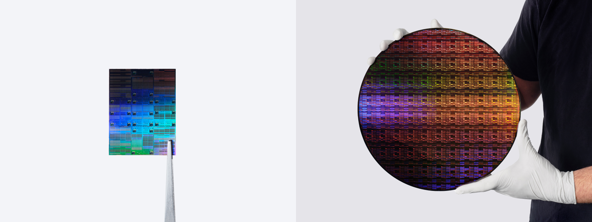
IBM’s 0.7-Nanometer Chip Technology Moves Closer to Reality With PDKs Planned for 2027
IBM is pushing deeper into the future of semiconductor manufacturing with its next-generation 0.7-nanometer chip technology, also known as 7-angstrom technology. The company has confirmed that it plans to make process development kits, or PDKs, available in the first quarter of 2027, giving chip designers an early opportunity to evaluate and prepare for the advanced manufacturing process.
The move marks an important step for IBM’s Nanostack technology, a chipmaking approach designed to improve transistor density, performance, power efficiency, and SRAM scaling. As the semiconductor industry moves beyond today’s leading 2-nanometer production nodes, companies are preparing for more advanced processes that use angstrom-based naming. Since 1 nanometer equals 10 angstroms, IBM’s 0.7-nanometer technology falls into the 7-angstrom class.
PDKs are essential tools for semiconductor design. They provide chipmakers with the technical rules, layout guidance, verification tools, and design scripts needed to build chips for a specific manufacturing process. These kits help companies test whether their future processors, accelerators, and memory designs can work effectively on a new node before the technology reaches broader availability.
For major chip designers working on CPUs, GPUs, AI accelerators, and other high-performance processors, early access to PDKs can be critical. It allows engineering teams to become familiar with the process, adapt their designs, and understand the potential benefits and limitations of a new manufacturing platform well ahead of commercial production.
IBM’s Nanostack technology takes a different approach to transistor organization by vertically stacking and staggering transistor structures. The goal is to save physical space while allowing better optimization of the two key transistor types used in modern chips: n-type and p-type transistors.
In simple terms, n-type transistors use materials that provide free electrons for conduction, while p-type transistors rely on electron vacancies. These two transistor types work together inside a chip to control electrical flow efficiently and prevent unnecessary power loss when circuits are idle.
Traditionally, the manufacturing requirements for n-type and p-type transistors are closely tied together, which can limit how much each can be optimized. IBM’s stacked approach separates them in a way that could open the door to new material choices and more refined tuning. This could help future chips achieve better performance and efficiency while reducing the amount of area needed on the silicon die.
One of the most important promises of IBM’s 7-angstrom technology is its potential impact on SRAM, a type of high-speed memory used directly on processors. IBM claims the technology could deliver up to 40% SRAM scaling, which would be a major breakthrough for advanced chip design.
SRAM scaling has become one of the biggest challenges in modern semiconductor manufacturing. While logic transistors in processors have continued to shrink with newer nodes, SRAM has not scaled as easily. When SRAM cell dimensions become extremely small, problems such as current leakage, power loss, signal integrity issues, and manufacturing variation become more difficult to control.
This matters because SRAM plays a critical role in modern processors, especially AI chips and graphics processors. It is used for on-die cache, helping compute units access data quickly without constantly reaching out to external memory. As AI workloads become larger and more demanding, chips need more cache, but adding SRAM takes up valuable die space.
In today’s high-performance AI accelerators, SRAM can consume a notable portion of the chip area. In some advanced GPU designs, cache and related SRAM structures may account for more than 10% of the total die. When additional cache is included inside compute blocks, that share can rise even further, competing with other major components for space.
This is why IBM’s SRAM scaling claims are especially significant. If Nanostack can reduce SRAM area while maintaining performance and power efficiency, future AI chips, data center processors, and high-performance computing products could pack more memory and logic into the same footprint. That could lead to faster processing, lower energy consumption, and more efficient chip designs.
The timing also matters. The semiconductor industry is entering a period where traditional scaling is becoming increasingly difficult and expensive. Manufacturers are no longer relying only on smaller transistor dimensions to improve chips. Instead, they are exploring new transistor architectures, advanced packaging, backside power delivery, stacked designs, and specialized materials.
IBM’s 0.7-nanometer Nanostack technology fits into this broader shift. Rather than simply shrinking everything in the conventional way, the approach aims to rethink how transistors are arranged and optimized. By stacking transistor types vertically and creating more design flexibility, IBM hopes to continue progress in chip scaling even as physical and electrical limits become harder to overcome.
Although the PDK release planned for early 2027 does not mean mass production is imminent, it is still a key milestone. PDK availability gives chip designers the chance to study the technology, begin early design exploration, and determine how future products might benefit from the new process.
If IBM’s 7-angstrom technology delivers on its promises, it could influence the next generation of processors used in artificial intelligence, cloud computing, consumer electronics, and high-performance computing. The potential combination of denser logic, improved power efficiency, and better SRAM scaling would be highly valuable as demand for faster and more energy-efficient chips continues to rise.
IBM has long played a major role in semiconductor research, and its latest progress with 0.7-nanometer technology shows that the race for advanced chip manufacturing is far from over. With PDKs expected in 2027, the industry is now one step closer to evaluating whether Nanostack can help define the future of ultra-advanced semiconductor design.