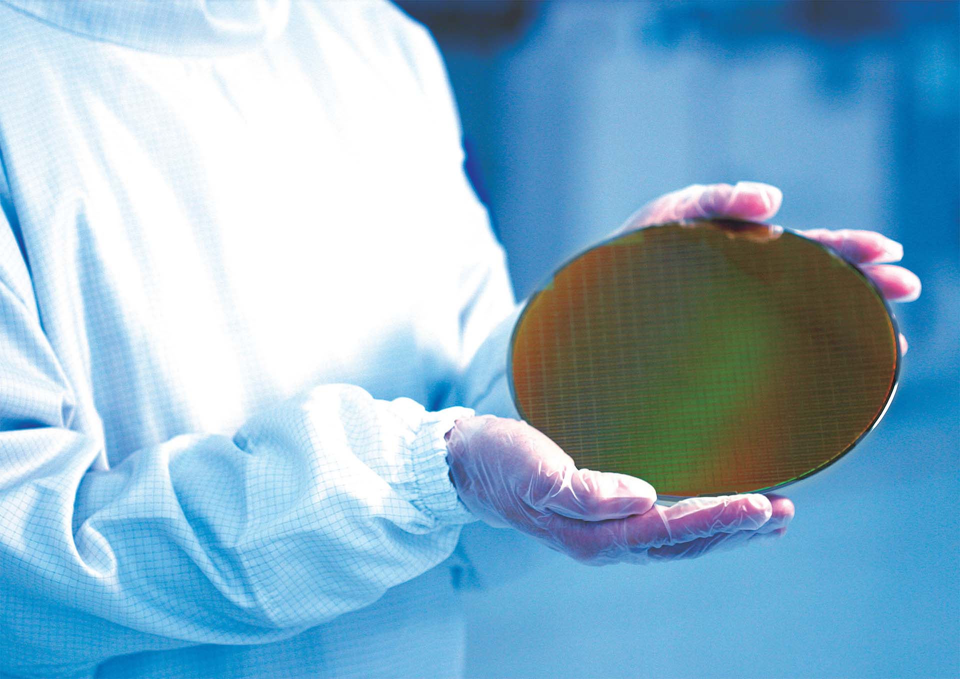
Samsung’s expanding chip manufacturing footprint in the United States is drawing fresh attention as demand for advanced production capacity keeps climbing. A new report suggests that Samsung Foundry is becoming one of the top destinations for fabless chip designers looking for a reliable U.S.-based manufacturing partner—especially as the industry grapples with tight supply and soaring AI-driven demand.
For years, most of the world’s leading chip designers leaned heavily on one primary foundry partner because capacity was generally available. That dynamic is changing fast. The ongoing AI boom has created a major bottleneck across advanced manufacturing nodes, pushing well-known companies like AMD, NVIDIA, Qualcomm, and Apple to seriously pursue a “dual-sourcing” strategy. In other words: keeping a primary supplier, while securing a strong secondary option to reduce risk and improve supply stability.
According to the report, Samsung is currently leading that race for secondary foundry business, with growing interest centered on its U.S. operations—particularly the Taylor, Texas facility. The Taylor fab is increasingly viewed as the next logical place to turn for companies that want cutting-edge semiconductor manufacturing in the United States.
One key reason Samsung is gaining momentum is customer confidence. The company’s foundry business has already tied itself to major names, including NVIDIA and Apple, which signals to other potential customers that Samsung can compete at the top end of the market. The report also indicates that companies like Qualcomm and AMD are exploring orders with Samsung, likely targeting Samsung’s 2nm-class process technologies (often referenced as SF2 and related variants).
Samsung’s timing may be working in its favor. Recent updates indicate the company is prioritizing the Taylor facility by shifting plans toward 2nm production and backing that move with investment in advanced packaging. That’s important because modern chip performance isn’t just about the manufacturing node—advanced packaging has become a major differentiator for AI and high-performance chips, enabling better power efficiency, bandwidth, and overall system performance.
Right now, many chip designers are searching for alternatives that can effectively complement or replace current leading-edge options. The report points out that, for customers looking beyond today’s most in-demand production capacity, the practical choices for advanced node alternatives appear limited to two major paths: Intel’s 18A and Samsung’s SF2. Both are positioned as higher-class node options, and the expanding interest in these technologies suggests the market is ready for more competition in advanced chip manufacturing.
That said, interest doesn’t automatically mean volume production is locked in. The report notes that the big milestone still ahead is converting customer discussions and plans into real foundry orders that show up on production lines. For Samsung and Intel alike, execution will be the next critical test as more chip designers aim to secure dual-sourcing agreements and stabilize long-term supply.
With U.S. chip investments accelerating and AI demand continuing to pressure the global supply chain, the fight to become the preferred secondary foundry is heating up—and Samsung’s Taylor fab appears to be a major focal point in what happens next.