Samsung’s 1000-Layer NAND Roadmap Could Bring 32 TB M.2 SSDs Closer to Reality
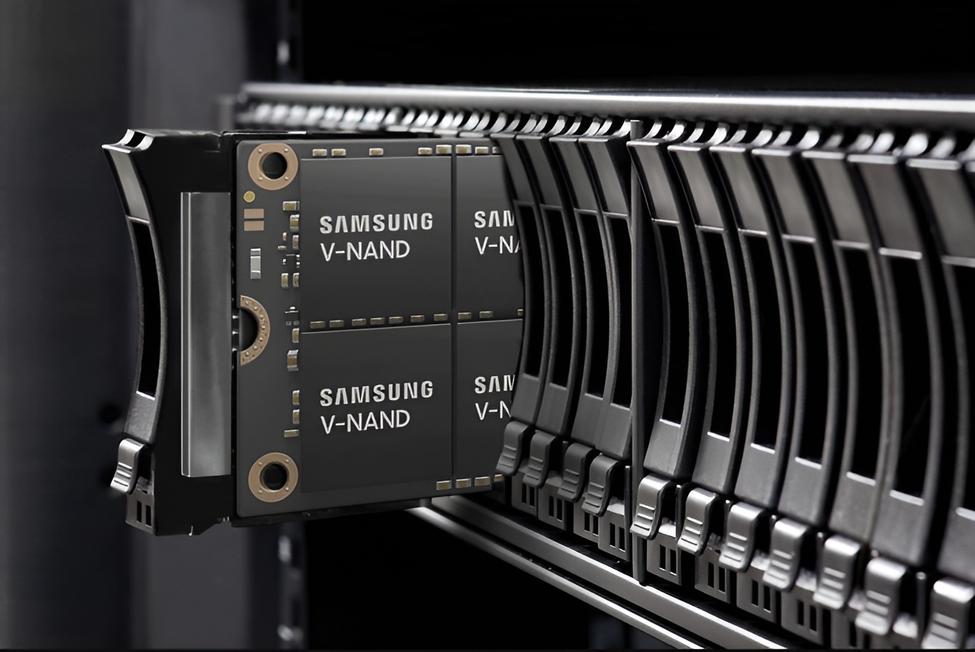
Samsung is preparing a major leap in SSD storage technology, with plans for next-generation NAND flash that could exceed 900 layers and eventually move beyond 1000 layers. The company’s future approach involves bonding two NAND stacks together, creating much denser memory chips designed for high-capacity solid-state drives.
The goal is simple but ambitious: deliver much larger SSD capacities without dramatically increasing the physical size of the drive. If successful, this technology could transform consumer and enterprise storage over the next decade, especially as demand grows from AI, cloud computing, data centers, gaming, and professional workloads.
Today, NAND manufacturers are entering the 400-layer era, but Samsung is already looking far beyond that. The company has outlined a roadmap that targets around 420-layer NAND by 2029 and more than 560 layers by 2030. After that, Samsung plans to push into the 900-layer and 1000-layer range by stacking and bonding multiple NAND structures together.
This kind of advancement could have a huge impact on SSD capacity. A future QLC M.2 SSD that currently tops out at around 8 TB could potentially scale to 32 TB using a similar compact form factor. That means future laptops, desktops, workstations, and compact servers may be able to store far more data without needing larger drives or multiple storage devices.
Samsung’s proposed solution is based on combining two 450-layer NAND stacks into one larger package. These two stacks would be connected using a bonding process known as Cell-Multi Bonding, or CMB. By joining two advanced NAND structures together, Samsung can significantly increase storage density while continuing to improve performance and efficiency.
However, building NAND chips with so many layers is not easy. As the number of layers increases, manufacturers face serious technical challenges. One of the biggest problems is wafer warping. When NAND stacks become taller and more complex, the wafer can bend or deform during manufacturing, making it harder to maintain accuracy and yield.
Samsung says it is working on solutions to address these issues. One important development is a new upper chuck design, which helps control warpage during production. The company is also improving overlay correction technology, which helps reduce alignment errors between layers. These improvements are essential for producing extremely tall NAND stacks with the precision needed for reliable SSDs.
The industry is currently racing to develop higher-layer NAND because storage demand is rising rapidly. AI training, generative AI services, cloud platforms, high-resolution video, gaming libraries, and enterprise databases are all consuming more storage than ever before. High-capacity SSDs are becoming increasingly important because they offer faster speeds, lower latency, and better energy efficiency than traditional hard drives.
Samsung is not alone in this competition. SK Hynix has already pushed forward with 321-layer NAND and is also working toward 400-layer technology. Different companies are exploring different bonding methods, including vertical bonding and hybrid bonding, to reach the next level of NAND density. These techniques will likely define the future of SSD manufacturing.
Chinese memory maker YMTC is also accelerating its NAND development. The company already produces 232-layer and 294-layer NAND products and is investing heavily in new fabrication capacity. As global demand for memory grows, especially due to AI-driven workloads, NAND suppliers are under pressure to expand output and improve density as quickly as possible.
The move toward 900-layer and 1000-layer NAND is still in the prototype and research stage, so these products are not expected to appear immediately. Samsung’s roadmap suggests that 400-layer NAND products will arrive first in the coming years, followed by 500-layer-class solutions around 2030. The 1000-layer generation is expected to become realistic sometime after that.
For everyday users, this technology could eventually mean affordable SSDs with much larger capacities. Instead of choosing between speed and storage space, future buyers may be able to get both in a single drive. Gamers could store massive game libraries, content creators could work with 8K video projects more easily, and professionals could keep larger datasets on local machines.
For data centers, the benefits could be even greater. Higher-density SSDs allow companies to store more data in the same physical footprint, reducing space requirements and potentially lowering power consumption. As AI workloads continue expanding, dense and efficient flash storage will become a key part of next-generation infrastructure.
Samsung’s 900-layer and 1000-layer V-NAND roadmap shows where the SSD market is heading: smaller drives, larger capacities, and more advanced manufacturing techniques. While there are still technical hurdles to overcome, the company’s progress in bonding technology, warpage control, and layer alignment suggests that ultra-high-capacity SSDs are moving from concept toward reality.
If Samsung can bring this technology to mass production, the next decade could deliver a major jump in storage capacity. A 32 TB M.2 SSD may sound extreme today, but with 1000-layer NAND on the horizon, it could become a normal option for high-end PCs, workstations, and data center systems in the future.