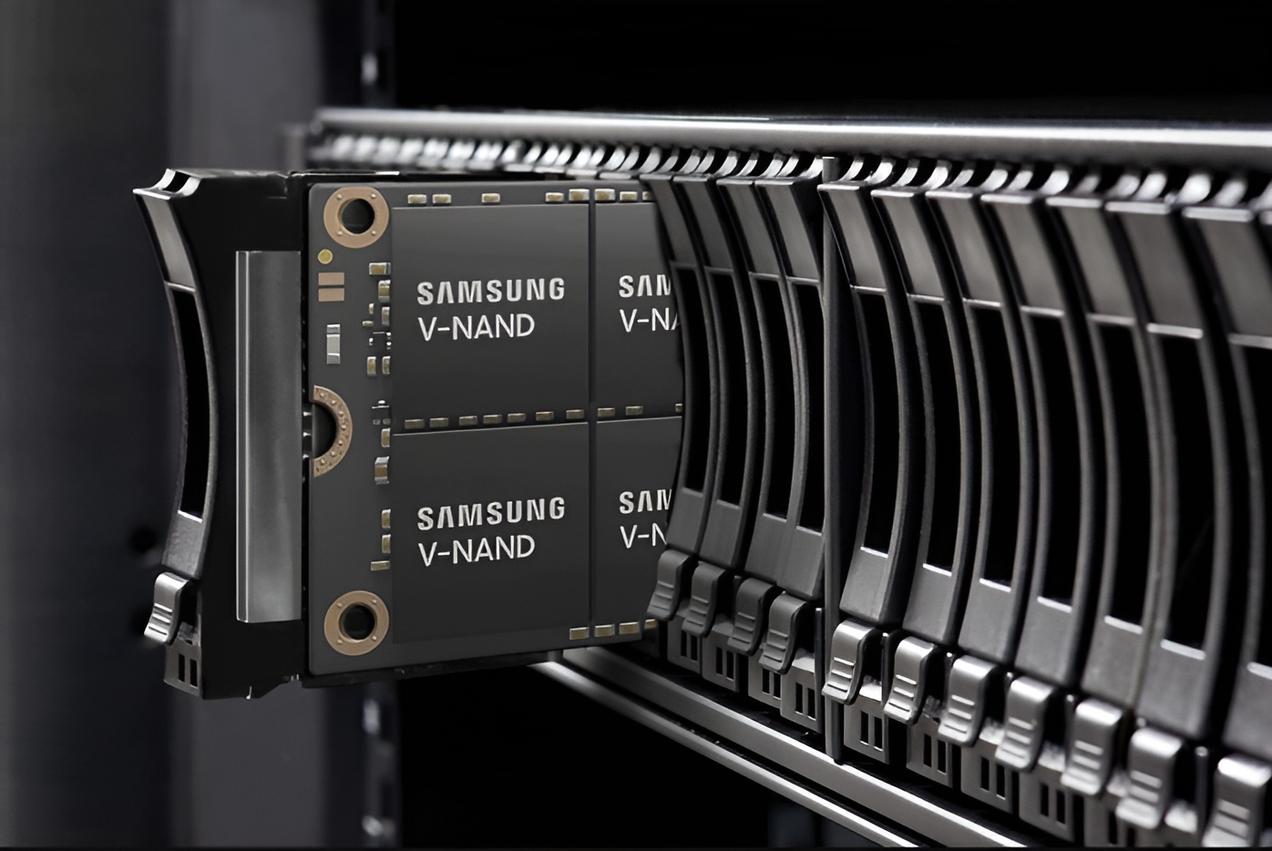
Samsung Moves Closer to 1000-Layer V-NAND With First 900-Layer Prototype
Samsung is taking another major step toward the future of high-capacity storage. The company has reportedly achieved its first 900-layer V-NAND prototype, bringing it significantly closer to its long-term goal of producing 1000-layer NAND technology.
The breakthrough highlights Samsung’s continued push to increase storage density, improve SSD capacity, and stay competitive in the rapidly advancing memory semiconductor market. As demand for faster and larger storage grows across servers, artificial intelligence systems, laptops, desktops, smartphones, and enterprise data centers, higher-layer NAND is becoming increasingly important.
Samsung’s 900-layer V-NAND prototype is said to use Cell Multi-Bonding, also known as CMB technology. This method bonds two 450-layer cell stacks together to create a single 900-layer structure. By stacking more memory cells vertically, Samsung can increase storage capacity without requiring a much larger physical footprint.
This approach could play a major role in the next generation of SSDs and embedded storage solutions. More layers generally mean higher storage density, which can lead to larger drives, improved efficiency, and potentially better cost-per-gigabyte over time.
Building NAND with this many layers is not simple. One of the biggest challenges Samsung had to overcome was wafer warping, a common issue when dealing with extremely tall memory stacks. To address this, the company reportedly introduced an improved upper chuck design to help stabilize the wafer during manufacturing.
Samsung also worked on reducing alignment problems between layers. At such high layer counts, even tiny positioning errors can affect production quality and yield. The company is said to have used overlay correction technologies to improve precision during the bonding process.
While the 900-layer design is still in the prototype phase, it represents an important milestone for Samsung’s V-NAND roadmap. The technology is not expected to appear in commercial products immediately, but it sets the foundation for future storage expansion.
The wider NAND industry is also moving quickly. SK Hynix has already developed 321-layer NAND technology and is working toward 400-layer products. Samsung is also expected to move into 400-plus-layer NAND in the coming years, using advanced bonding techniques to continue increasing density.
Competition is also intensifying from China’s YMTC, which has been accelerating its NAND development. The company already offers 232-layer and 294-layer NAND products and is investing heavily in new manufacturing facilities. These expansions could significantly increase wafer output at a time when demand for storage is rising due to AI workloads, cloud infrastructure, and high-performance computing.
Samsung’s progress with 900-layer V-NAND shows how quickly the memory market is evolving. The company has previously explored next-generation materials, including ferroelectric-based approaches, as part of its plan to eventually reach 1000-layer NAND.
For consumers and businesses, this race could lead to larger and more efficient SSDs in the future. Enterprise servers may benefit from higher-capacity drives for AI training, cloud services, and large-scale databases. Consumer devices could also see more compact storage options with greater capacity, helping laptops, desktops, and smartphones handle increasingly data-heavy applications.
Samsung’s 1000-layer V-NAND technology is currently expected around the end of the decade, with 400-layer and higher products arriving before then. Although the 900-layer prototype is not yet ready for mass production, it is a strong sign that ultra-high-layer NAND is no longer just a concept.
As storage demand continues to climb, Samsung’s latest prototype could become a key stepping stone toward the next era of SSD and flash memory technology.