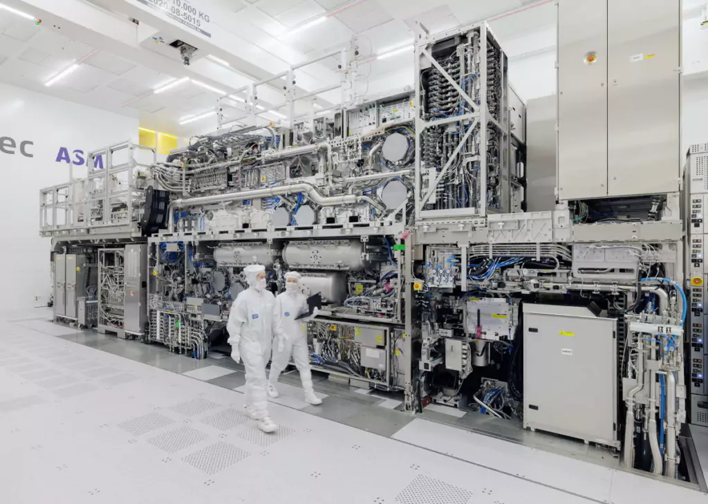
Samsung is poised to elevate the semiconductor industry competition as it gears up to integrate its first state-of-the-art High-NA EUV lithography machine within the next quarter. This move signals a crucial step in semiconductor technology, enabling chipmakers to sharpen their edge in a fiercely competitive market.
Traditionally, the adoption of High-NA EUV lithography equipment has been a hallmark of leading semiconductor manufacturers, with rivals like Intel and TSMC already making significant headway in securing similar tools. Samsung, however, is not far behind its competitors and is expected to receive this next-generation equipment from ASML—an esteemed name in the semiconductor industry.
Reports indicate that Samsung is on track to acquire the high-performing Twinscan EXE:5000 High-NA lithography machine from ASML. This machine stands out for its remarkable 8nm resolution and utilization of a 13.5nm EUV light wavelength, allowing for the fabrication of notably smaller chips with up to 1.7 times higher precision and increased transistor densities by approximately 2.9 times. The Twinscan EXE:5000 is acclaimed for its industry-leading productivity rates, which suggests that Samsung’s semiconductor production capabilities will likely see substantial advancements.
The introduction of this new equipment into Samsung’s arsenal holds great potential for the semiconductor landscape. The Korean tech titan plans to station the first batch of High-NA machinery at their Hwaseong Campus, dedicated to research and development. The exact timing of the commercial deployment of this advanced lithography tool remains to be solidified, as the intricacies involved in setting up such complex machinery are non-trivial. Nevertheless, the projection is that Samsung might have the High-NA equipment operational by late 2025, barring any unforeseen challenges.
The expansion of High-NA technology amongst titans like Intel, TSMC, and now Samsung is likely to drive further growth in the semiconductor markets. Intel has already shared intentions to deploy High-NA for its 14A node, and TSMC aims to apply it to its future 2nm nodes. While Samsung’s specific plans for the use of High-NA technology have yet to be officially unveiled, it’s anticipated that they will align with industry trends, potentially incorporating High-NA into their inaugural 2nm process technology.
This development is a testament to the ongoing enhancements and commitments to innovation within the semiconductor industry, promising to set new benchmarks in chip performance and production efficiency. As these tech giants continue to invest in cutting-edge lithography, the trajectory for more powerful and streamlined electronics looks promising.