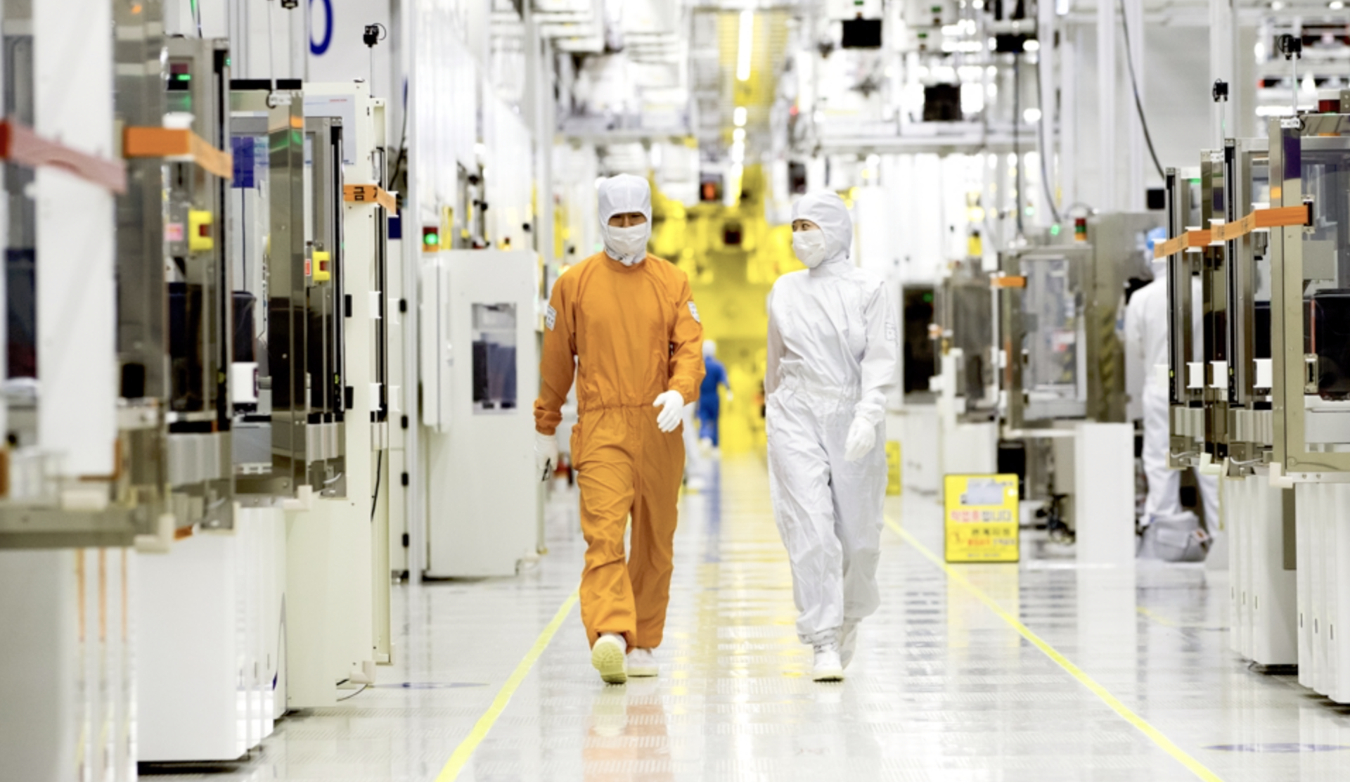
Samsung Eyes High-NA EUV Lithography for 1nm Chip Production by 2030
Samsung is preparing to bring high-NA extreme ultraviolet lithography into its semiconductor manufacturing roadmap as the company works toward producing chips on a 1-nanometer process node. According to comments from Samsung Electronics Vice President of Technology ChangMin Park, the company expects high-NA EUV tools to become essential for future chipmaking technologies, particularly starting with the A10 generation, commonly associated with 1nm-class manufacturing.
The move highlights Samsung’s long-term push to stay competitive in advanced semiconductor fabrication, where smaller transistors, improved power efficiency, and higher performance are critical goals. If Samsung’s roadmap stays on track, chips built using 1nm-class technology could enter mass production around 2030.
Why high-NA EUV matters for next-generation chips
Modern chip manufacturing depends heavily on lithography, the process used to print tiny circuit patterns onto silicon wafers. As chipmakers continue shrinking transistor sizes, they run into physical limits tied to the wavelength of light used in lithography systems.
Today’s EUV lithography systems use light with a wavelength of 13.5 nanometers. While this has enabled major progress in advanced chip production, manufacturing at even smaller process nodes requires more precise patterning. That is where high numerical aperture, or high-NA, EUV technology becomes important.
High-NA EUV machines use more advanced lens systems with a higher numerical aperture, allowing them to print finer circuit patterns with greater accuracy. The latest high-NA EUV systems feature a 0.55NA lens design, compared with the lower aperture used in current EUV tools.
For chipmakers, this can reduce the need for complex multi-patterning techniques. Multi-patterning requires the same layer of a chip to be exposed multiple times, which adds cost, increases production complexity, and raises the risk of defects. High-NA EUV can help simplify the process by enabling smaller features to be printed more directly.
Samsung delays high-NA EUV use until 1nm-class nodes
Samsung had previously expected to apply high-NA EUV lithography to earlier advanced nodes, including 2nm and 1.4nm-class technologies. However, Park indicated that the company now sees high-NA EUV becoming necessary from the 1nm generation onward.
This suggests that Samsung may continue using existing EUV methods, along with other patterning improvements, for its near-term 2nm and 1.4nm production plans. The decision reflects the broader industry challenge of adopting high-NA EUV tools, which are extremely complex, expensive, and still progressing toward full production maturity.
Although high-NA EUV machines have already begun shipping to major semiconductor companies, full-scale adoption remains gradual. These tools are among the most advanced manufacturing systems ever built, with enormous size, high installation requirements, and a need for extensive calibration before they can be used in commercial chip production.
A major step in Samsung’s 1nm semiconductor roadmap
Samsung’s plan to introduce high-NA EUV for 1nm chips shows how important the technology is expected to become in the next phase of semiconductor scaling. In chip manufacturing, 1 nanometer equals 10 angstroms, which is why future process nodes are often discussed using angstrom-class naming.
At these dimensions, even tiny improvements in lithography precision can have a significant impact on performance, power consumption, and manufacturing yield. For Samsung, successful high-NA EUV adoption could help strengthen its position in the global foundry market, where it competes to produce advanced chips for smartphones, artificial intelligence processors, data centers, and high-performance computing.
The semiconductor industry has long relied on Moore’s Law, the trend of increasing transistor density over time. While progress has become harder and more expensive, high-NA EUV is viewed as one of the key tools that could help chipmakers continue advancing beyond today’s leading-edge process technologies.
What this means for the chip industry
Samsung’s decision points to a cautious but strategic approach. Instead of rushing high-NA EUV into earlier production nodes, the company appears to be waiting until the technology becomes more refined and economically practical for mass production.
This could help Samsung reduce risk while still positioning itself for the next major leap in chip fabrication. By the time 1nm-class manufacturing is ready near the end of the decade, high-NA EUV systems may be more mature, better optimized, and more suitable for high-volume output.
If successful, Samsung’s use of high-NA EUV could lead to more powerful and efficient processors across multiple industries. From AI accelerators and mobile chips to automotive processors and cloud computing hardware, 1nm-class semiconductors could play a major role in the next generation of digital technology.
Samsung’s latest roadmap makes one thing clear: high-NA EUV is not just an experimental tool for the future. It is becoming a central part of advanced chip manufacturing, and Samsung expects it to be critical when the industry reaches the 1nm era.