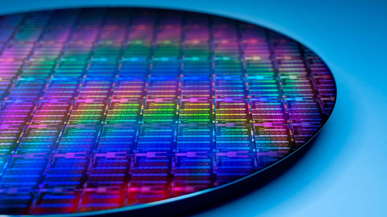
Moore’s Law may not be racing ahead the way it did in the 2000s, but chip technology isn’t standing still. A newly shared semiconductor roadmap from IMEC, the Belgium-based research and innovation center known for shaping future manufacturing directions, outlines how the industry could reach sub-1nm process nodes in the next decade and push far beyond that in the 2040s.
The big takeaway: the path to 0.7nm is real, but it’s not immediate. According to the roadmap, the first sub-1nm logic node is projected around 2034, with even more aggressive “angstrom-class” nodes (below 0.2nm) appearing on long-term research timelines around 2046. These dates reflect when technologies could be development-complete, not necessarily when consumers will see them in mass-produced chips.
Why shrinking is harder now than it used to be
From roughly 1998 to 2010, logic density scaling was extremely strong, with SRAM area effectively halving at a rapid pace. Since 2010, however, improvements have shifted toward more incremental, near-linear gains. In other words, the industry can still advance, but each step is more difficult and more expensive.
One major reason is cost. As chipmakers push into the angstrom era, the tools and manufacturing steps needed to print and build smaller features become dramatically more expensive. At the same time, the industry has found other ways to keep performance improving without relying solely on smaller transistors. Chiplet-based designs and advanced packaging have become central, letting companies mix and match different silicon blocks and scale compute in a more flexible and cost-effective way.
That said, packaging isn’t a magic solution. Power delivery, heat, and overall system cost can become limiting factors, especially for AI and high-performance computing, where memory bandwidth and close chip-to-memory integration are critical.
The sub-2nm era: nanosheets and Gate-All-Around transistors
The roadmap highlights the transition from FinFETs to nanosheet-based Gate-All-Around (GAA) transistors as the key shift for the next generation. Nanosheets improve control over current leakage and help boost performance and efficiency as traditional scaling gets tougher.
This nanosheet/GAA era begins with 2nm-class technologies and continues through several “angstrom” nodes leading toward approximately 1.0nm around 2031 (often referenced as A10 in angstrom naming). That A10-class point is positioned as the final major stop for nanosheet scaling before the industry needs a bigger architectural change to keep transistor density climbing.
Sub-1nm starts around 2034: CFET goes vertical
To move below 1nm, the roadmap points to CFET (Complementary FET) technology. CFET builds on nanosheet ideas but stacks transistor types vertically, rather than placing them side-by-side. That vertical stacking is crucial because it cuts cell area and can deliver a major density jump when 2D shrinking becomes less effective.
Key milestones described in the roadmap include:
– Around 2034: A7 (0.7nm) using CFET, marking the first projected sub-1nm node
– Around 2036: A5 (0.5nm)
– Around 2040: A3 (0.3nm)
As CFET matures, the roadmap suggests CMOS transistor density gains that can reach roughly 80% compared to prior approaches, depending on implementation and design rules.
Beyond CFET: 2D materials and the “2 angstrom” era
Past 2040, the roadmap shifts from mostly device-architecture evolution to a combination of architecture plus fundamentally new materials. That’s where 2D FETs appear.
The concept is that transistor channels could be made from ultra-thin 2D materials rather than conventional silicon structures, enabling continued density scaling at dimensions where traditional approaches struggle.
IMEC’s roadmap places:
– Around 2043: A2 (0.2nm) as an early 2D FET milestone
– Around 2046: sub-A2 nodes (below 0.2nm), extending 2D approaches even further
This is highly research-oriented and could shift significantly based on breakthroughs, manufacturing readiness, and economics.
Wiring (BEOL) becomes just as important as transistors
Shrinking transistors alone doesn’t solve performance if the “wires” that connect them can’t keep up. The roadmap also details BEOL (Back-End-of-Line) scaling, which covers interconnect materials and methods.
Today’s mainstream interconnect approach relies heavily on copper with damascene processes at roughly 24–26nm metal pitch. The roadmap shows continued refinement through about 2028, then a transition toward new techniques and materials to reduce resistance and improve efficiency as dimensions tighten.
Notable shifts include:
– Moving from copper toward ruthenium (Ru) as nodes approach 1nm-class and below, alongside intentional air gaps and self-aligned vias to cut resistance and improve signal integrity
– For 0.5nm-class and beyond, exploring alternate metals and advanced conductors such as epitaxial PtCoO₂ (platinum cobalt oxide) on sapphire to achieve extremely low resistance at very tight pitches (down into roughly 16nm to 12nm ranges in the roadmap’s projections)
This focus on interconnects is essential because, at advanced nodes, performance and power are often limited by wiring resistance and heat rather than transistor switching alone.
Power delivery is also being redesigned: IVRs move closer to the chip
Another part of the roadmap looks at power technology through the early 2030s, with a clear trend: bring voltage regulation closer to the processor package to improve efficiency and reduce losses.
The roadmap describes steps where integrated voltage regulators (IVRs) move from the motherboard into the PCB near the chip, and then increasingly into the package itself. This approach helps manage conversions such as 48V down to 12V, and then down to sub-1V levels (around 0.8V), which modern logic requires.
Packaging-level power integration is also tied to next-generation capacitor and silicon power device concepts, complementing the rise of 2.5D and 3D integration where compute, memory, and interposers are tightly coupled.
What this means for AI chips, HPC, and the next decades of silicon
The bigger message behind the roadmap is that “Moore’s Law” is evolving rather than ending. Traditional shrinking is harder, slower, and costlier, but the industry has multiple levers to keep improving performance and efficiency: vertical transistor architectures like CFET, new channel materials via 2D FETs, major interconnect changes, and aggressive 3D packaging and power delivery integration.
If this roadmap holds even roughly true, the next 10–20 years of chips won’t be defined by transistor size alone. They’ll be shaped by how well manufacturers can combine advanced nodes with smarter packaging, better wiring, and more efficient power delivery to meet the exploding demands of AI workloads and high-performance computing.