Samsung’s push toward next-generation high-bandwidth memory could be hitting an important speed bump. New information from Korea suggests Samsung may not move into mass production of its latest 1d (also referred to as D1d) DRAM technology anytime soon, after failing to reach the yield levels needed to justify full-scale manufacturing.
Yields matter because they directly impact cost, reliability, and profitability. Even if a chip technology is technically ready on paper, mass production only makes sense when enough usable dies come off the line to deliver a solid return on investment. In this case, Samsung’s 1d DRAM is reportedly producing results below internal targets, raising concerns that a trial run—and especially large-volume production—could be financially risky.
The report notes that Samsung’s 1d DRAM had already cleared a pre-production approval stage, but the company is now said to be re-evaluating the process roadmap to improve yields before committing to mass production. As a result, the timing for restarting or ramping production is unclear and may be postponed indefinitely until the technology meets performance and efficiency goals in the fab.
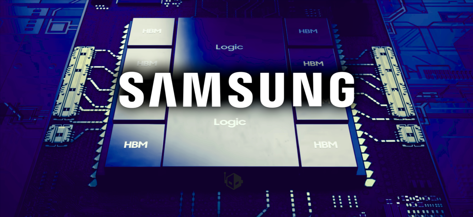
This is a big deal because 1d DRAM is expected to be a key building block for Samsung’s future HBM roadmap. It’s widely anticipated to play an important role in HBM5E, which is projected to be the company’s ninth-generation high-bandwidth memory product. HBM is crucial for AI accelerators and data center GPUs, where memory bandwidth and power efficiency can heavily influence real-world performance.
Right now, Samsung’s existing 1c DRAM is the foundation across multiple upcoming HBM generations, including HBM4, HBM4E, and HBM5. Industry expectations are that HBM4 will begin rolling out later this year and will be paired with next-wave AI hardware platforms from major GPU vendors. HBM4E is expected to extend that momentum with even higher performance variants, while HBM5 and custom designs are positioned to power future accelerator lineups and competing solutions.
It’s also worth noting the difference between moving fast in development versus being ready for mass production. Samsung has reportedly been working to shorten its HBM development cycle, which can help the company prepare new designs more quickly. But faster development doesn’t automatically solve manufacturing bottlenecks—especially if yields remain too low for stable, cost-effective output. In other words, the lab schedule can improve, but the factory still has to deliver.
To strengthen its manufacturing capabilities, Samsung is also investing in expanded production infrastructure. The company is building a large semiconductor facility in Onyang, South Korea, described as spanning roughly the area of four soccer fields. The site is expected to support next-generation DRAM and HBM output through back-end operations such as packaging, testing, logistics, and quality control—steps that are just as critical as wafer processing when it comes to delivering consistent high-volume memory products.
All of this is unfolding as competition in the HBM market intensifies. Rivals are pushing aggressively to secure supply agreements with leading AI companies, and the winners will likely be the ones that can combine advanced memory technology with dependable yields, scalable production, and a clear path to profitability. In that context, Samsung’s next move will likely depend on how quickly it can raise 1d DRAM yields to target levels—because in the HBM race, production readiness is just as important as innovation.