As global AI compute demand keeps climbing, chipmakers are racing to secure enough high-bandwidth memory (HBM) to feed today’s data-hungry GPUs and accelerators. That surge is now creating a fast-growing ripple effect in a less-talked-about corner of the semiconductor industry: advanced inspection, testing, and failure analysis equipment—especially high-end microscopy systems used to detect defects, confirm process quality, and speed up troubleshooting.
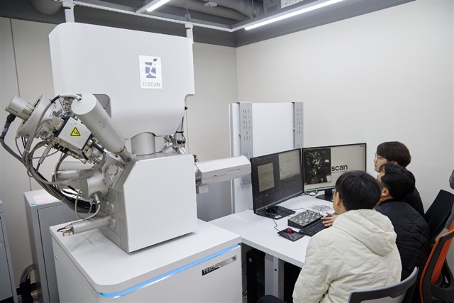
HBM is far more complex than traditional memory because it relies on stacked dies, ultra-dense interconnects, and tighter packaging tolerances. When you stack multiple layers and push bandwidth and thermal limits, even small imperfections can turn into major yield losses. That’s why HBM production is driving increased demand for integrated microscopy platforms designed specifically for semiconductor inspection. These systems help engineers analyze micro-defects, identify failure points, and validate manufacturing improvements without wasting weeks on trial-and-error iterations.
The emphasis isn’t just on buying more tools—it’s also on building faster, closer support. With HBM output becoming a strategic priority, the industry is placing new value on localized service hubs that can keep critical inspection equipment running with minimal downtime. When every batch matters and every delay is expensive, having maintenance, calibration, and expert support available locally can make a measurable difference in yield control and production speed.
This market shift is affecting the entire semiconductor ecosystem. Memory manufacturers are scaling up failure analysis capacity to protect margins and meet strict customer requirements. Foundries and packaging specialists are also becoming more reliant on deep inspection capabilities as advanced packaging and chiplet-style designs expand. At the same time, equipment suppliers that offer integrated microscopy platforms and strong regional service networks are finding themselves in higher demand as the AI supply chain tightens.
Ultimately, the HBM boom is turning inspection and failure analysis into competitive advantages. Companies that can quickly detect defects, reduce costly rework, and improve yields are better positioned to secure long-term AI supply agreements. As AI hardware continues to expand across data centers and edge devices, demand for HBM testing and semiconductor microscopy tools is set to remain a major driver shaping the next phase of the semiconductor inspection equipment market.