Samsung and SK hynix are taking two very different paths toward next-generation DRAM memory, according to industry insiders—and the stakes couldn’t be higher. As AI data centers keep expanding, demand for high-performance memory has surged, tightening supply across HBM, DRAM, and related chips. Because many of these products depend on the same raw materials and manufacturing capacity, the entire memory market is feeling the squeeze. Now, the race is on to develop the production method that could define the future of DRAM.
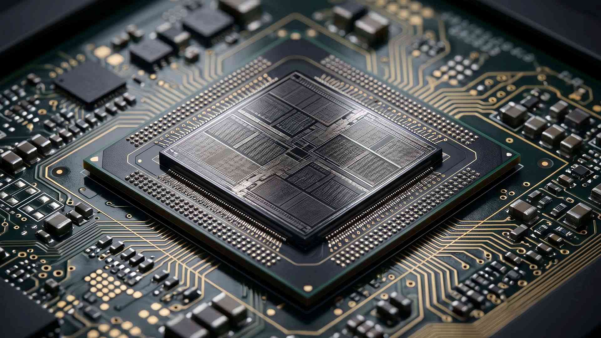
Unlike application processors, where manufacturing advances are typically described in nanometers, memory makers use a different naming system. DRAM process generations are often labeled with codes such as “1c,” which generally points to increasingly advanced nodes in the 10nm class and beyond. But shrinking memory technology isn’t as straightforward as scaling logic chips, because DRAM isn’t just about transistors—it also needs capacitors to store data.
Each DRAM cell relies on a transistor working in tandem with a capacitor. As manufacturers push to smaller nodes, maintaining a capacitor that can reliably hold a charge becomes more difficult. The capacitor has to remain large enough to function, but smaller geometries make that harder to achieve without running into design and manufacturing constraints. This is one of the major reasons the industry is exploring new DRAM architectures, including more three-dimensional designs that can boost density without forcing everything into an increasingly cramped 2D footprint.
One reported direction under consideration at Samsung borrows a concept from NAND flash manufacturing. Sources suggest Samsung is interested in applying gate-all-around FET (GAAFET) technology to future DRAM chips. In logic manufacturing, GAAFET improves transistor control by wrapping the gate around the channel, increasing gate contact and enhancing performance and efficiency.
But using GAAFET in DRAM introduces a new challenge: DRAM cells still need capacitors, so Samsung would have to integrate a GAAFET-based transistor together with a capacitor inside each memory cell. To make that possible—and to improve density—one technique said to be on the table is shifting certain circuitry beneath the memory array. This “circuit-under-array” style layout is commonly associated with NAND, where placing control circuitry below the main array helps free up surface area for storage.
SK hynix, meanwhile, is reportedly pursuing a different strategy based on what’s described as a 4F²-style approach. In this concept, transistors are stacked vertically, and the gate material wraps around them in a way that echoes the benefits of gate-all-around designs. In addition, key components involved in handling data from the capacitor are positioned beneath the transistor pillar, aiming to improve efficiency and scaling as DRAM becomes more complex.
What makes this more than just an engineering contest is the long-term impact. Insiders suggest both companies are pushing to have their approach recognized first, hoping it becomes the standard blueprint for next-generation DRAM manufacturing. If one design direction becomes the dominant model, it could shape performance, cost, yields, and competitiveness across the memory industry—especially at a time when AI infrastructure is turning high-bandwidth and high-density memory into one of the most valuable pieces of modern computing.