OpenAI has revealed a fresh direction for future AI hardware in a newly published patent that outlines an advanced chip design built around chiplets and a lot more high-bandwidth memory (HBM) than today’s typical packages can support.
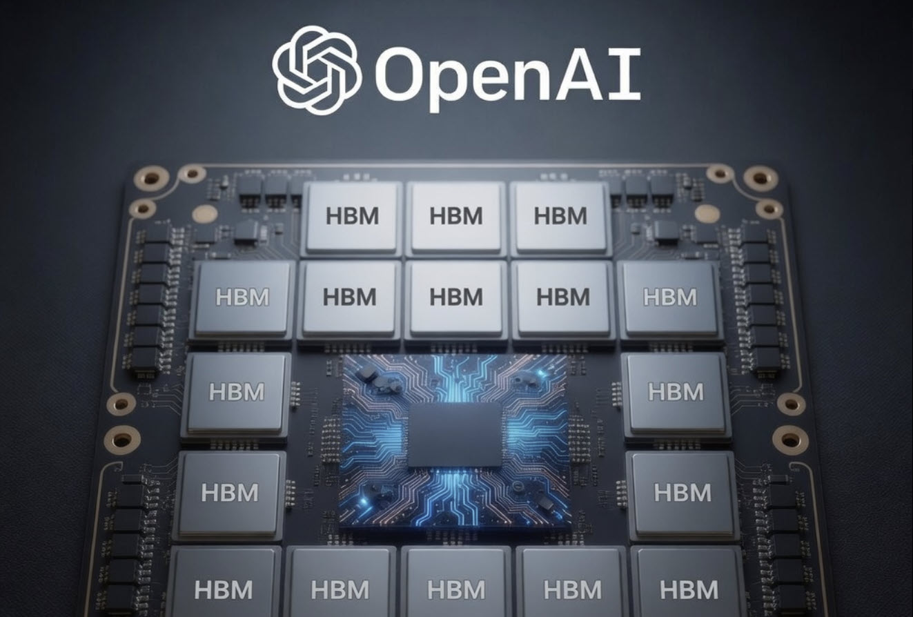
The patent, titled “Non-Adjacent Connection of High-Bandwidth Memory Chiplets, I/O Chiplets, And Compute Chiplets Through Embedded Logic Bridges,” describes an approach where multiple compute chiplets sit on a single package and are surrounded by numerous HBM memory stacks. The key idea is using embedded logic bridges to connect everything together, allowing high-speed communication even when the chiplets aren’t placed right next to one another.
Why does this matter for AI? Modern AI workloads—especially training and running large models—depend heavily on fast access to huge pools of memory. HBM provides extremely high bandwidth, but getting lots of HBM onto the same package alongside compute is difficult with current packaging rules and physical constraints.
One major limitation comes from how HBM is typically integrated today. HBM stacks communicate with other parts of the package through metal routing on the base layer, and current industry standards generally require HBM to be adjacent to the compute chiplet. There’s also a practical distance cap: the metal connections are expected to stay under about 6mm from the PHY controller on the primary chiplet. That tight spacing makes it hard to scale to a large number of memory stacks.
OpenAI’s patent proposes embedded logic bridges as a way around this. These bridges can extend the workable distance from roughly 6mm out to around 16mm, which opens the door to placing HBM stacks farther away while still maintaining high-speed connectivity. The bridges can also do more than simply pass signals along. According to the patent, they may take on tasks such as acting like an HBM controller for a stack or delivering high-speed PHY functionality for chiplet-to-chiplet communication within the same package.
The design also points to a modern die-to-die (D2D) connection approach that aligns with the UCIe (Universal Chiplet Interconnect Express) standard—an industry push to make chiplets from different sources communicate more easily and efficiently inside advanced packages.
In one example configuration highlighted in the patent, OpenAI describes a compute chiplet connected to as many as 20 HBM memory stacks using embedded logic bridges. That stands out because traditional approaches often top out around four, six, or eight HBM stacks depending on the package and design constraints. If a chip can truly scale to that many stacks, the memory capacity and bandwidth increases could be significant—exactly the kind of upgrade that makes next-generation AI systems faster and more capable, especially as model sizes keep growing.
This concept also overlaps with real-world advanced packaging work already happening in the industry. Intel, for example, has an established technology known as EMIB (Embedded Multi-Interconnect Bridge), built to enable high-density connections between chiplets using small embedded bridges rather than full interposers. Approaches like this are designed to expand chip capabilities, simplify certain packaging challenges, and push beyond the reticle limits associated with some interposer-based designs.
The big takeaway is that OpenAI’s patent signals serious interest in custom AI silicon designs that scale compute and memory together—particularly by using chiplet-based architectures and advanced packaging to break past today’s HBM placement limits. Whether this results in a production chip and which manufacturing partners or packaging technologies might be used isn’t confirmed by the patent itself, but the direction is clear: more chiplets, more HBM, and better ways to connect them for high-performance AI.