TSMC’s CoPoS packaging could reshape next-generation AI chips by 2028
TSMC is reportedly preparing a major leap in advanced chip packaging with its next-generation CoPoS technology, which is expected to enter mass production in the second half of 2028. The new packaging approach could play a key role in the future of high-performance AI accelerators, where demand for larger, more powerful chip packages continues to rise.
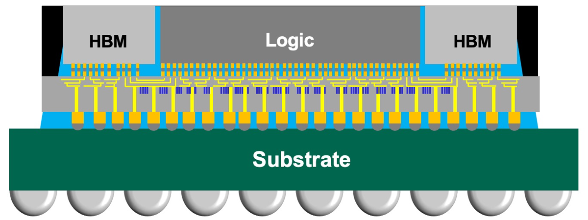
Analyst Ming-Chi Kuo says CoPoS, short for chip-on-panel-on-substrate, is designed to move beyond the limits of TSMC’s current CoWoS, or chip-on-wafer-on-substrate, packaging technology. CoWoS has become essential for advanced AI chips because it allows processors, high-bandwidth memory, and other components to communicate at extremely high speeds inside a single package.
However, as AI chips grow more complex, the physical limits of existing packaging methods are becoming harder to ignore.
Why CoPoS matters for AI chip development
Modern AI processors are not just single chips. They are advanced packages that combine GPUs, memory stacks, and other silicon components into one tightly connected system. The more powerful the AI chip, the more space is often needed for these components.
TSMC’s current CoWoS technology uses a silicon interposer, which acts as a high-speed bridge between the GPU and memory. This approach has worked well for today’s leading AI accelerators, but it is constrained by the size limits of lithography equipment. In simple terms, the tools used to create the interposer restrict how large the final package can become.
CoPoS aims to solve this problem by removing the need for a traditional interposer. Instead, it uses larger panels that can support much bigger chip packages. According to Kuo, this could allow TSMC to build packages more than nine times larger than the standard reticle-size class used in lithography.
That extra space could be critical for future AI processors, especially as companies push for greater computing power, more memory capacity, and improved energy efficiency.
NVIDIA may be among the first adopters
Kuo suggests that NVIDIA could be one of the earliest customers for TSMC’s CoPoS technology. The company’s future Feynman AI chips have been mentioned in connection with next-generation packaging options, including both TSMC’s upcoming CoPoS and Intel’s EMIB-T packaging technology.
The rapid growth of AI data centers has made advanced packaging one of the most important areas in semiconductor manufacturing. While chip process nodes still matter, packaging is now just as vital because it determines how efficiently multiple chip components can work together.
For companies developing large AI accelerators, the ability to fit more compute and memory into a single package can directly affect performance. This is why TSMC’s CoPoS roadmap is drawing attention across the semiconductor supply chain.
How TSMC’s CoPoS packaging is expected to work
According to Kuo, TSMC’s CoPoS technology will use glass in two important ways.
First, glass will be used as a temporary carrier during early chip assembly. This helps support the chip components while they are being placed and processed.
Second, the final substrate will reportedly include a glass core sandwiched between layers of Ajinomoto Build-up Film, commonly known as ABF. ABF is widely used in advanced substrates because it supports fine wiring patterns and high-density chip connections.
Kuo also clarified that CoPoS does not use a glass interposer. Instead, the chips are attached to the ABF layer of the substrate. This distinction is important because some early discussions around the technology may have confused the glass core substrate with a glass interposer.
By using a panel-based approach rather than a wafer-based interposer, CoPoS could offer better economics for extremely large chip packages. That means it may not only enable larger designs but also help make them more practical to manufacture at scale.
Mass production expected in the second half of 2028
Kuo’s latest timeline points to CoPoS entering mass production in the second half of 2028, which is earlier than some previous expectations. If that schedule holds, the technology could arrive just in time for the next major wave of AI chip architectures.
This timing is significant. AI workloads continue to become more demanding, and companies building large language models, robotics platforms, autonomous systems, and cloud AI infrastructure will need increasingly powerful hardware. Advanced packaging technologies such as CoPoS could become a major factor in meeting that demand.
TSMC is already a dominant force in high-end semiconductor manufacturing, and its CoWoS capacity has been under heavy demand due to the AI boom. CoPoS could strengthen its position further by offering customers a path to larger and more capable AI chip designs.
The bigger picture for semiconductor packaging
The semiconductor industry is entering an era where performance gains are no longer driven only by shrinking transistors. As Moore’s Law becomes harder and more expensive to maintain, chipmakers are relying more heavily on advanced packaging to improve performance.
Technologies like CoWoS, CoPoS, and EMIB-T are part of this broader shift. Instead of building one massive chip, companies can combine several specialized components into a single advanced package. This approach can improve yield, reduce design complexity, and deliver higher overall performance.
For AI hardware, this is especially important. High-bandwidth memory needs to sit close to the processor to reduce latency and improve data transfer speeds. Larger packages also allow more memory stacks and compute units to be integrated together.
TSMC’s CoPoS technology appears to be designed for that future: larger packages, better scalability, and improved manufacturing economics for ultra-high-performance AI chips.
If mass production begins in 2028 as expected, CoPoS could become one of the most important packaging technologies for the next generation of AI accelerators. Its use of a glass-core ABF substrate and panel-based manufacturing approach may help chip designers move beyond today’s size limitations and create more powerful processors for the rapidly expanding AI market.