TSMC is moving faster on its next big advanced packaging push as demand for AI GPUs and high-performance computing chips continues to surge. The company is reportedly accelerating the rollout of CoPoS, a packaging approach that shifts part of the manufacturing process away from traditional round wafers and toward larger rectangular glass panels.
The move could become an important step for the semiconductor industry, especially as AI chipmakers face growing pressure to deliver more powerful processors in higher volumes. Advanced packaging has become just as critical as chip fabrication itself, because modern AI accelerators rely on tightly integrated compute dies, memory stacks, and interconnects to achieve better performance and efficiency.
Unlike conventional wafer-based packaging, CoPoS uses larger panel formats that can offer more usable surface area. In theory, this allows manufacturers to package more chips at once, helping improve production capacity and reduce bottlenecks. For AI GPUs and HPC processors, where chip packages are becoming larger and more complex, that extra space could make a major difference.
Supply chain sources indicate that the first wave of demonstration equipment for TSMC’s CoPoS process has started moving into the early rollout phase. These tools are expected to help validate the production flow, test panel handling, and prepare suppliers for future volume manufacturing.
The timing is significant. Demand for AI hardware remains extremely strong, with cloud providers, data center operators, and enterprise customers all investing heavily in accelerated computing. As a result, chip packaging capacity has become a key constraint across the industry. TSMC has already been expanding its advanced packaging technologies, and CoPoS appears to be part of a broader strategy to support the next generation of AI and HPC chips.
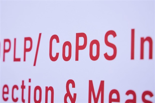
The shift to rectangular glass panels is not a simple change. Panel-level packaging requires new equipment, materials, and process controls. Glass panels must be handled with precision to avoid warping, cracking, or alignment issues during production. Suppliers will also need to adapt inspection, bonding, lithography, and assembly tools for the new format.
Still, the potential benefits are substantial. If TSMC can successfully scale CoPoS, the technology may help improve throughput for large chip packages and ease pressure on existing advanced packaging lines. This could be especially important as future AI processors become even larger and require more memory bandwidth, more chiplets, and more sophisticated interconnect designs.
For the semiconductor market, TSMC’s faster CoPoS rollout signals that advanced packaging innovation is becoming a central battleground. The race is no longer only about making smaller transistors. It is also about how efficiently companies can connect multiple chips together inside a single powerful package.
Over the next several years, CoPoS could play an important role in supporting the growth of AI infrastructure, data center acceleration, and high-performance computing. While the technology is still in its early stages, the arrival of demo equipment suggests that TSMC and its supplier network are preparing for a major transition in chip packaging production.