NVIDIA’s next-generation Feynman GPUs are shaping up to be a major turning point for data center hardware, largely because they’re now expected to be the company’s first GPUs to ship with Co-Packaged Optics (CPO). That’s a notable shift from earlier expectations, where CPO commercialization was viewed as something that would take much longer to reach real-world deployment.
Co-Packaged Optics, often discussed under the broader umbrella of silicon photonics, aims to reduce dependence on traditional copper connections by using light to move data. The idea is straightforward but powerful: optical links can move enormous amounts of information with lower latency and fewer limitations over distance, especially compared to copper. In modern AI infrastructure, where clusters continue to scale out and compute nodes may be spread across facilities, those distances can stretch to 10 kilometers or more. At that scale, moving data at several hundred gigabits per second becomes increasingly difficult with conventional interconnect approaches—exactly the problem CPO is designed to solve.
Earlier roadmaps suggested CPO wouldn’t be commercially ready until around 2033. Now, that timeline appears to have accelerated dramatically. The latest details indicate NVIDIA has pulled that plan forward by roughly five years, targeting 2028 for CPO debut alongside the Feynman GPU platform. That matters for anyone tracking AI factory design, because the interconnect layer is quickly becoming one of the biggest bottlenecks in training and inference at scale.
Industry momentum around optical interconnect standards is also building. A major multi-company effort called the Optical Compute Interconnect Multi-Source Agreement (OCI-MSA) was established in March, bringing together several top names across AI hardware and platforms, including NVIDIA, Broadcom, AMD, Meta, OpenAI, and Microsoft. With NVIDIA positioned as the dominant supplier in AI accelerators, its decision to introduce a co-packaged optical solution with Feynman could influence how quickly the broader ecosystem moves toward optical-first interconnects.
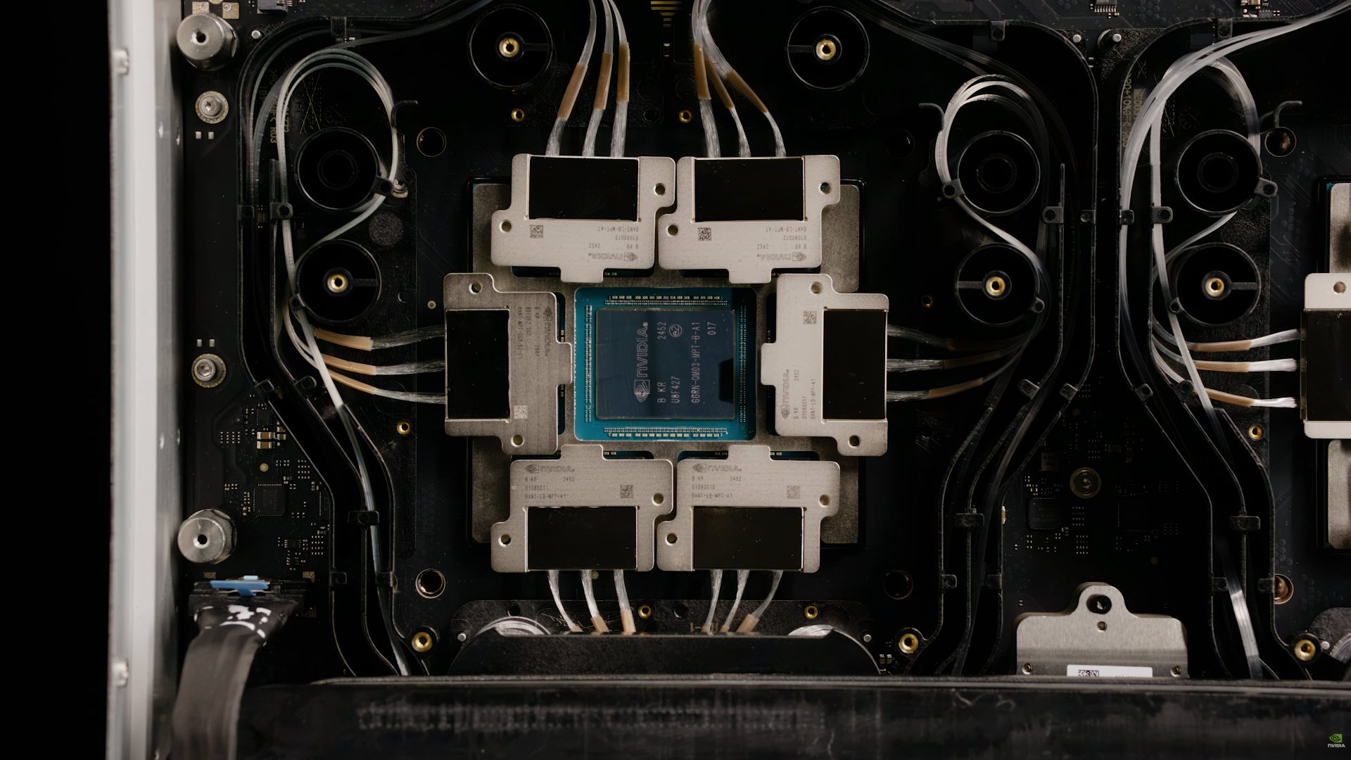
Feynman isn’t only about optics, either. NVIDIA has also confirmed the architecture will adopt 3D die stacking technology. That opens the door to significant design changes, including the possibility of stacked GPU dies—an approach that can improve density, bandwidth, and potentially performance-per-watt, depending on how it’s implemented.
Manufacturing and packaging choices will be a big part of the story as well. NVIDIA is reportedly planning to use Intel as a foundry partner and take advantage of advanced packaging technologies such as EMIB. Advanced packaging has become one of the most important competitive levers in modern high-performance computing, especially as chiplets, stacked dies, and complex memory subsystems become the norm.
Memory is another area where NVIDIA is signaling something different. Rather than simply listing “next-gen HBM,” the Feynman platform is now associated with custom HBM technology. With Rubin expected to use HBM4 and Rubin Ultra expected to use HBM4E, the “custom HBM” reference for Feynman suggests NVIDIA may be working with an enhanced version of HBM4E or potentially a custom HBM5-class solution. Either way, the message is clear: memory bandwidth and power efficiency remain central priorities, and NVIDIA wants a configuration that stands out from standard, off-the-shelf HBM roadmaps.
NVIDIA is also introducing a new data center CPU architecture to pair with Feynman. Instead of relying on Vera, the Feynman platform is expected to use a brand-new CPU called Rosa, named after American physicist and Nobel Prize winner Rosalyn Sussman. Specific technical details haven’t been shared yet, but given NVIDIA’s recent trajectory with tightly integrated CPU-GPU platforms, Rosa is likely being designed to better support next-generation AI data movement, scheduling, and platform-level efficiency.
Beyond GPU and CPU changes, NVIDIA plans to keep expanding the broader hardware stack around its AI platforms. The pipeline includes components such as BlueField-5, NVLink 8 with CPO, Spectrum 7 204T with CPO, and CX10—highlighting that optics won’t be limited to a single product, but may become a recurring theme across networking and interconnect technologies as NVIDIA pushes toward larger, faster AI clusters.
The current expectation is that NVIDIA’s Rosa + Feynman data center solutions will arrive in 2028. Competition won’t be standing still, either: AMD is also reported to be working on its own co-packaged optics efforts with GlobalFoundries, with a first implementation expected around the same timeframe alongside MI500-class GPUs.
For anyone watching the future of AI infrastructure, the big takeaway is that optical interconnects are no longer a distant concept. NVIDIA’s accelerated CPO plans for Feynman suggest the industry is moving faster to solve the bandwidth and latency challenges that come with AI systems operating at massive scale—and 2028 is now shaping up to be a key year for that transition.