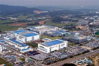
Nvidia is reportedly stepping up its preparations for its next wave of AI and data center GPUs by taking a closer look at Samsung Electronics’ advanced semiconductor packaging operations in South Korea. According to recent reports, Nvidia has made multiple visits in quick succession to Samsung’s packaging campus in Cheonan, a move that suggests the company is actively verifying key parts of its next-generation high-bandwidth memory roadmap.
These visits are being viewed as a strong signal that qualification and supply chain checks for upcoming HBM memory are moving into a more serious phase. In the AI hardware world, HBM is one of the most critical ingredients for performance. It feeds modern GPUs with the massive bandwidth needed for training and running large AI models, and small improvements in memory speed, capacity, and packaging can translate into major real-world gains in throughput and efficiency.
Industry watchers believe the focus is tied to next-generation HBM, including HBM4, and how it will be packaged and integrated for Nvidia’s future GPU platforms, widely expected to include the Rubin generation. The packaging side is especially important because high-bandwidth memory is not just about the DRAM itself. It depends heavily on advanced integration technologies that connect stacked memory to the GPU with extremely high-density interconnects, tight tolerances, and robust thermal and power delivery characteristics. A memory stack can be fast on paper, but it still needs to meet stringent reliability and manufacturability demands when deployed at scale in high-power accelerators.
Samsung has been pushing to expand its position in the HBM market, where competition has grown intense as demand from AI servers continues to surge. For Nvidia, the stakes are equally high: securing reliable HBM supply and validating packaging capabilities early can help reduce risk, stabilize production ramps, and avoid bottlenecks that could limit availability of next-gen GPUs.
The reported frequency of Nvidia’s visits stands out because it implies more than casual check-ins. In semiconductor manufacturing terms, repeated on-site reviews often align with auditing production readiness, reviewing quality control processes, evaluating packaging yields, and confirming that partners can deliver consistent volume when a new platform moves closer to launch. With AI accelerators relying on complex multi-chip packaging and increasingly advanced memory stacks, ensuring that every link in the supply chain is ready has become a competitive advantage.
If these reports are accurate, Nvidia’s increased attention to Samsung’s packaging operations may also hint at broader supplier diversification efforts. With HBM demand growing rapidly and supply often tight, GPU makers and hyperscale customers alike have been looking for ways to secure capacity, qualify additional sources, and strengthen resilience across the memory ecosystem.
For readers tracking the future of AI GPUs, HBM4, and the next major platform after Blackwell, this is an important development to watch. It underscores how the race for AI performance isn’t only happening in GPU architectures and silicon nodes, but also in the behind-the-scenes world of memory packaging, qualification, and supply chain execution—where the winners are often decided long before products reach the market.