NVIDIA’s plans for its GTC 2026 keynote may be even bigger than many expected, with new reporting suggesting the company could use the stage to preview its next-generation Feynman chips. If that happens, GTC 2026 could offer an early look at the hardware NVIDIA believes will help define the next era of AI and accelerated computing.
NVIDIA has already been signaling that this year’s keynote is meant to “set the tone for the next decade of computing,” and CEO Jensen Huang has teased technology that has “never [been] unveiled before.” That has fueled growing speculation that Feynman will finally step into the spotlight publicly at GTC 2026, potentially giving developers, enterprise customers, and the wider tech industry their first official glimpse of what comes after the current roadmap.
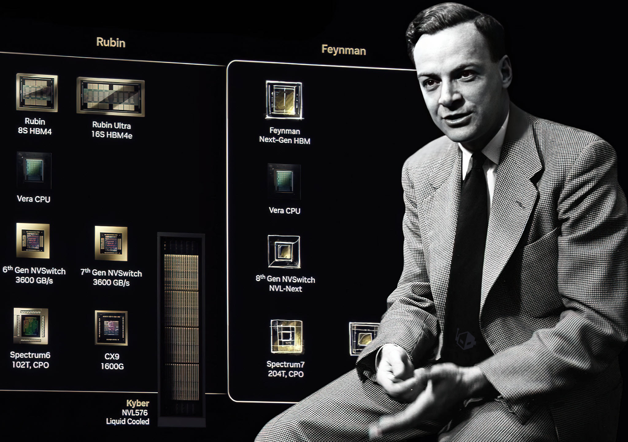
While concrete technical details remain scarce, one key point stands out: Feynman is expected to be among the first chips built on TSMC’s A16 (1.6nm) manufacturing technology. This node is described as a substantial semiconductor leap, incorporating Super Power Rail (SPR) and pushing toward what’s being positioned as the smallest process technology in the world. The report also indicates NVIDIA could be TSMC’s first—and possibly only—customer for A16 during the early high-volume manufacturing period, since other categories (like mobile) may need more extensive architectural changes before adopting it.
Beyond the manufacturing node, Feynman may carry another important shift: a stronger focus on latency reduction. As AI workloads evolve, raw throughput isn’t the only priority—latency is increasingly critical for real-time inference, interactive AI, and responsiveness at scale. That’s where speculation about Groq-style LPU (Language Processing Unit) integration enters the picture. The idea is that NVIDIA could explore bringing LPU units into the package as part of a broader hybrid approach, potentially using advanced bonding methods similar in spirit to the stacking strategies seen in other parts of the industry. If NVIDIA does pursue an on-package LPU option with Feynman, it could improve latency-sensitive performance, but it would also likely make design complexity and manufacturing significantly more challenging.
If NVIDIA follows its familiar playbook, the Feynman segment at GTC 2026 may resemble past next-gen previews: a high-level architecture overview, a discussion of expected capabilities, and guidance on mass-production timing. Based on current expectations, Feynman production may not begin until around 2028, which could place customer shipments in the 2029–2030 window, depending on NVIDIA’s rollout strategy and how the platform is positioned across data center AI, cloud deployments, and enterprise infrastructure.
GTC 2026 is set to begin on March 15 and will take place in San Jose, California. If Feynman does make its debut there, it could become one of the most closely watched announcements in NVIDIA’s recent history—especially as the AI hardware race shifts from simply being bigger and faster to being smarter, more efficient, and dramatically lower in latency.