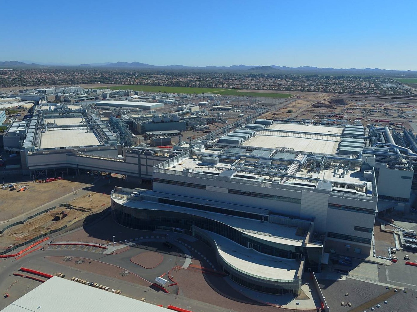
Intel’s next big manufacturing step, the 14A process node, is shaping up to be more ambitious—and more expensive—than 18A. Company finance chief David Zinsner confirmed the jump in cost is driven by next‑generation High‑NA EUV lithography tools that run about $380 million each, a sharp increase over today’s roughly $235 million systems. The payoff: a process tuned for efficiency and performance that’s also the first Intel node designed from the ground up to serve both Intel’s own products and outside foundry customers.
What 14A brings to the table
– Performance-per-watt uplift of roughly 15–20 percent versus 18A
– Power consumption reduced by about 25–35 percent
– RibbonFET 2 transistors for improved drive current and scaling
– PowerDirect backside power delivery to cut resistive losses and improve voltage droop
– Turbo Cells to squeeze out higher performance within tight power envelopes
– High‑NA EUV single-exposure resolution down to 8 nm features, compared to about 13.5 nm with current tools
That High‑NA EUV capability is the headline change. Finer features in a single exposure can reduce multi-patterning complexity, sharpen critical dimensions, and ultimately improve yield and variability—key factors for both leading-edge CPUs and custom silicon.
The business reality: 14A needs customers
Intel’s foundry push hinges on external demand. While internal products will tap 14A, the company needs third‑party designs to justify the node’s higher capital costs. If the pipeline falls short, Intel could slow-roll or even shelve 14A. Leadership says confidence is rising thanks to improving 18A yields, but 2026 is viewed internally as the pivotal year to judge 14A’s momentum.
Strategic guardrails are also in place. Intel Foundry cannot be spun off under current U.S. government contract terms that require Intel to retain at least 51 percent control—an important constraint as the company courts outside customers.
Why Intel will still lean on TSMC
Despite its aggressive internal roadmap, Intel plans to keep using external fabs where it makes sense. According to Zinsner, the mix today is roughly 70 percent in‑house and 30 percent outsourced. TSMC reportedly builds the entire Lunar Lake lineup and most Arrow Lake chips, and Intel is said to be among the first customers lined up for TSMC’s 2 nm node, expected to produce future Nova Lake processors. In other words, multi‑sourcing remains central to Intel’s product cadence and risk management.
Fuel for the roadmap
Intel has attracted significant funding to push its manufacturing agenda forward, including about $2 billion from SoftBank and $5.7 billion in government support, with additional investments anticipated from Mobileye (around $1 billion) and Altera (about $3.5 billion). On the product side, Panther Lake on 18A is slated to enter production later this year, setting the stage for how quickly 14A follows.
The bottom line
14A isn’t just about more speed—it’s about dramatically better efficiency, advanced power delivery, and a manufacturing platform designed to welcome outside customers. If Intel secures enough foundry wins and keeps yields trending up, 2026 could mark the transition from promise to production. Until then, expect Intel to balance its own fabs with strategic use of TSMC to keep the product pipeline moving.