Elon Musk has pulled the curtain back on what he’s calling one of the most important projects in his orbit: TeraFab, a mega-scale chip manufacturing plan he believes can shape the “future of civilization.” It’s a huge claim, but the details he’s shared make it clear he’s aiming far beyond a typical semiconductor fab. Musk’s end goal is straightforward in concept and extreme in execution: produce so much compute that today’s global chip output looks insignificant by comparison.
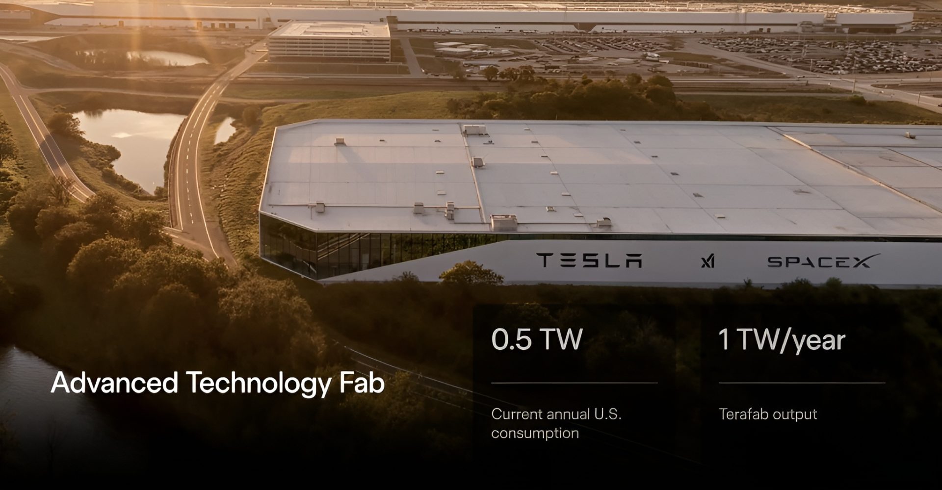
At the core of Musk’s pitch is a staggering production target. He says TeraFab is designed to deliver about 1 terawatt of compute output per year, spanning logic chips, memory, and advanced packaging. If that sounds more like a power plant than a factory, that’s the point—Musk is framing compute as the key resource for the next era of AI, autonomy, robotics, and space infrastructure. He also argues that all chip manufacturing on Earth today only meets about 2% of the compute demand he wants to reach, positioning TeraFab as the missing engine needed to close that gap.
One of the most attention-grabbing elements is the starting point: TeraFab is expected to focus on 2nm-class production from the beginning. That would place it among the most advanced manufacturing targets in the industry, right out of the gate, rather than ramping up through older nodes first. While many chip projects require years of gradual escalation, Musk’s plan suggests a leap straight into leading-edge territory.
TeraFab also leans heavily on a manufacturing philosophy Musk describes as “rapid, recursive improvement.” Instead of splitting chip development across separate organizations and facilities, he wants everything integrated into unified production lines: chip design, fabrication, testing, packaging, and even mask creation and refinement. The idea is to compress the feedback loop so dramatically that engineers can iterate faster—design a mask, make the chip, test the chip, refine the mask, and repeat—all under one roof. Musk’s argument is that this tight loop would allow the fab to improve itself continuously, unlocking speed advantages that conventional, distributed chip development can’t match.
Location-wise, the project is planned for Austin, Texas, aligning it near Tesla’s headquarters and existing infrastructure. Musk has also framed it as a joint effort pulling together talent and objectives across Tesla, SpaceX, and xAI, all of which are hungry for compute for different reasons—self-driving and robotics, AI model training and inference, and space systems that increasingly rely on onboard intelligence.
Then there’s the most unconventional part of the plan: Musk says most of the compute won’t stay on Earth. He claims around 80% of TeraFab’s compute would ultimately be deployed in space, arguing that Earth’s power constraints and deployment limits make it difficult to scale to the levels he wants. In his vision, space-based compute can take advantage of solar energy, and heavy-lift launches would move hardware into orbit at massive scale. It’s an idea that ties directly into his “galactic civilization” narrative, where compute becomes foundational infrastructure for space expansion rather than something confined to terrestrial data centers.
As for what TeraFab would actually produce first, Musk points to Tesla’s next-generation AI5 chips as an immediate priority. These are described as the chips intended for key Tesla initiatives such as Full Self-Driving, Robotaxi, and Optimus humanoid robots. That AI5 demand would represent the approximate 20% portion of compute he expects to remain ground-based.
The remaining 80% of space-focused compute, according to Musk, would come from a new class of chips called D3. He describes these as custom-designed units intended for orbital AI satellites, built to function in harsher environments and likely engineered to handle unique challenges such as thermal control and reliability in space conditions. In short, AI5 appears aimed at Tesla’s near-term product roadmap, while D3 is positioned as a backbone technology for an orbital compute layer.
Musk also acknowledged the role of current chip partners, expressing gratitude toward major suppliers across the existing semiconductor ecosystem. At the same time, he argues that the pace at which those partners are willing or able to expand is far lower than what his companies need. In his view, building TeraFab isn’t about replacing suppliers out of preference—it’s about capacity and speed. He’s essentially saying demand has outgrown what the traditional scaling curve can deliver.
Of course, the ambition is exactly what makes the project controversial. Semiconductor manufacturing is famously difficult to scale, not only because building a fab is expensive, but because the supply chain that supports leading-edge production is complex and capacity-constrained. Experts often point to bottlenecks such as the global availability of advanced lithography tools and the long timelines required to bring new wafer capacity online. Achieving the output Musk describes would likely require extreme vertical integration, flawless execution, and sustained access to the most advanced equipment in the world.
Another big question still hanging in the air is how exactly TeraFab would secure its process technology. There’s talk that Tesla could pursue a licensing approach for 2nm production, potentially involving a partnership structure, though nothing is confirmed. Until more concrete details emerge—tooling orders, build timelines, capacity plans, and process ownership—TeraFab sits in that familiar Musk zone: part engineering proposal, part moonshot, and part strategic signal to the market.
What’s clear is that Musk is trying to redefine how people think about chips. Instead of semiconductors as components that feed products, he’s pitching semiconductors as civilization-scale infrastructure—the resource that determines how quickly AI and robotics advance, and how far space-based industry can go. Whether TeraFab becomes a working reality at the scale promised or not, it’s already forcing a bigger conversation about compute supply, energy limits, and where the next generation of AI hardware might ultimately live.