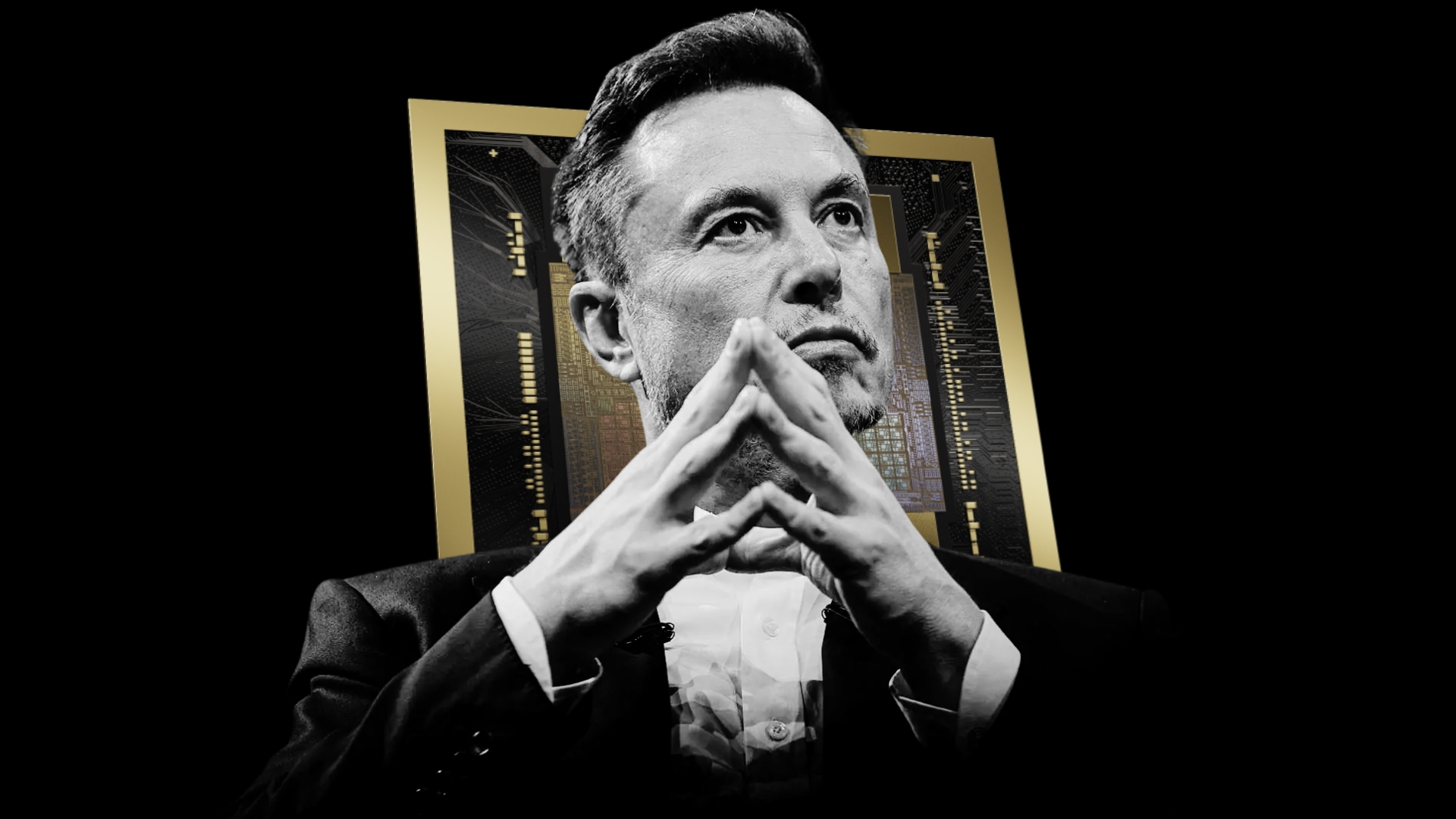
Tesla’s newly revealed TeraFab initiative is shaping up to be one of the boldest semiconductor manufacturing plays the industry has seen in years—and it’s already sparking talk of an intensifying fight for top engineering talent. With Elon Musk publicly setting sky-high expectations for the facility, Tesla now appears to be looking to Taiwan as a key place to recruit the specialized experts needed to turn the concept into reality.
At the center of the plan is a staggering production goal: TeraFab is envisioned to deliver as much as 1 terawatt of compute per year. Tesla has even floated an unusual deployment split, with roughly 80% of that compute intended for Earth-based needs and 20% aimed at space-focused use cases. While many semiconductor veterans remain skeptical of a target this extreme, the latest reports suggest Tesla is pressing ahead—starting with people.
Recruiting efforts are reportedly focused on experienced foundry engineers in Taiwan, including professionals currently working for leading chipmakers in the region. If Tesla follows through aggressively, it could ignite a fresh “talent war” in one of the world’s most strategically important semiconductor hubs—especially at a time when seasoned process and manufacturing experts are already hard to find globally.
Tesla’s own hiring activity also points to serious intent. One notable opening tied to TeraFab seeks a Module Process Engineer with the kind of background typically associated with advanced foundry development. The role emphasizes speeding up advanced system-on-chip (SoC) progress and calls for deep familiarity with modern transistor architectures such as gate-all-around (GAA) and FinFET. It also lists a high bar for experience—more than a decade in foundry or process development—signaling that Tesla isn’t looking for generalists, but for proven experts who have been close to cutting-edge node transitions.
So what might TeraFab actually build first? Based on current chatter, early efforts could target 2nm-class manufacturing, positioning the project in the same next-generation arena that other major national semiconductor efforts are chasing. Even so, the bigger challenge may not be raw scale at the start. For an initial facility, the smarter—and more realistic—path would be to prove stable process technology, strong yields, and repeatable manufacturing performance before attempting anything close to the massive compute-output goal Musk has described.
Another detail raising eyebrows is the suggested scope. TeraFab is expected to go beyond wafer fabrication into advanced packaging and memory-related capabilities. That combination dramatically increases the range of specialized skills required—process integration, materials expertise, packaging workflows, yield engineering, and more—making the hiring challenge even more complex and potentially disruptive to the broader labor market in semiconductors.
Then there’s the money. One recent analyst estimate puts the potential cost of TeraFab at up to $5 trillion when modeled against today’s equivalent for 1TW compute capacity. The analysis compares high-end AI hardware supply chain requirements and concludes that achieving the scale Tesla is talking about could demand investment so enormous it would dwarf typical industry spending—an eye-popping figure that fuels both curiosity and doubt.
For now, the clearest signal is Tesla’s recruiting posture. Pursuing elite chip talent—particularly from Taiwan—suggests that internal teams are treating TeraFab as more than a speculative idea. Still, major questions remain unanswered, from technical feasibility to timelines, supply chain constraints, and how Tesla would manage the unprecedented scale it’s implying. Until the company provides concrete engineering and operational details, TeraFab will continue to sit in a strange space: part ambitious roadmap, part industry-shaking rumor, and part headline-grabbing spectacle.