China’s CXMT could soon gain access to domestically made DUV lithography machines, a move that may strengthen the country’s semiconductor supply chain and accelerate the company’s ambitions in next-generation memory production.
Following a blockbuster public market debut that sparked intense investor interest, CXMT is reportedly among the first Chinese semiconductor companies expected to receive locally produced deep ultraviolet lithography equipment this year. The deliveries are said to come from Shanghai Yuliangsheng Technology, a China-based firm that has entered the DUV lithography market with plans to build five machines this year and increase production to around 20 units next year.
CXMT is expected to be one of the earliest recipients, alongside major Chinese chipmakers such as SMIC and Hua Hong. That placement highlights the strategic importance of CXMT in China’s broader push to reduce reliance on foreign semiconductor equipment and build a more self-sufficient chip manufacturing ecosystem.
The reported lithography systems are believed to be 28nm immersion DUV machines. Most components are said to be sourced domestically, although some critical parts may still come from Japan. Even so, the development marks an important step for China’s semiconductor industry, especially as access to advanced foreign lithography tools remains restricted.
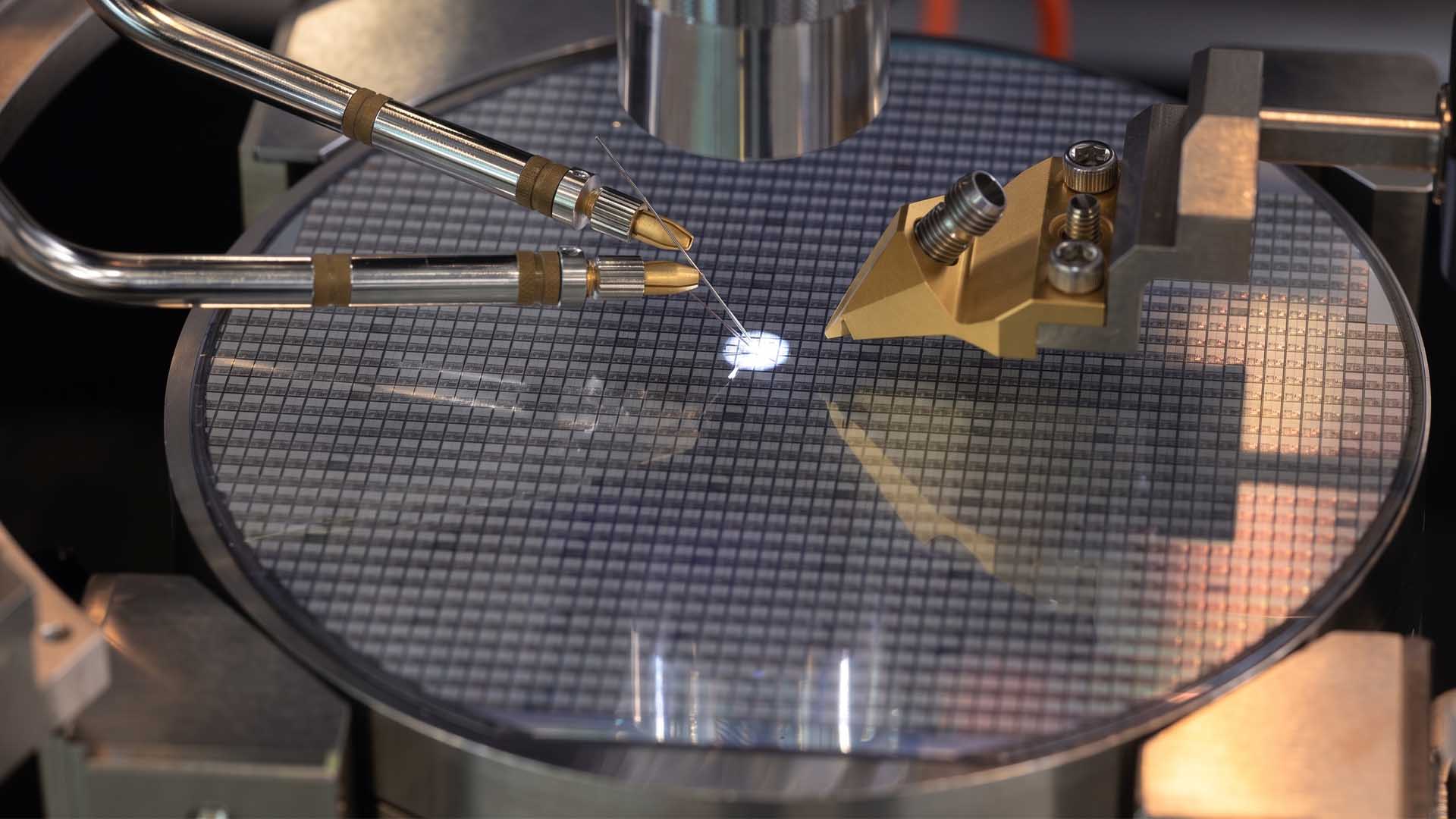
DUV lithography plays a crucial role in chip manufacturing. It uses deep ultraviolet light, typically generated by argon fluoride lasers at a wavelength of 193 nanometers, to print tiny circuit patterns onto silicon wafers. While DUV is not as advanced as extreme ultraviolet lithography, chipmakers can still use techniques such as multi-patterning to create much smaller and more complex features than a single exposure would normally allow.
For companies unable to access EUV machines, DUV remains essential. When combined with advanced process strategies such as design technology co-optimization, DUV can help manufacturers improve yields, reduce layout errors, and push existing equipment further. This is particularly important for Chinese chipmakers looking for alternative paths to produce more advanced semiconductors despite export controls.
For CXMT, domestic DUV access could be especially valuable. The company is moving quickly to expand production after its high-profile IPO, with shares reportedly surging nearly 500 percent by the end of its first trading session. The fresh capital is expected to support an aggressive capacity expansion plan, with CXMT aiming to raise output from about 200,000 wafers per month to roughly 300,000 wafers per month by the end of this year.
The company is also building two new fabrication plants in Shanghai and Hefei. Once completed, these facilities could lift CXMT’s total production capacity to around 600,000 wafers per month. If its expansion proceeds as planned, CXMT could become one of the world’s most important DRAM producers and may even challenge Micron in production volume by the end of the decade.
At present, CXMT is mass-producing 1a DRAM using its G5 process node. However, because the company does not have access to EUV lithography systems, it is focusing heavily on next-generation 3D DRAM. Instead of relying primarily on shrinking horizontal chip features, 3D DRAM stacks memory structures vertically to increase storage density and capacity.
This approach could allow CXMT to improve memory performance and density without depending on the most advanced EUV-based manufacturing processes. By using argon fluoride immersion DUV systems to pattern certain horizontal layers and then stacking them vertically through advanced bonding methods, CXMT may be able to create high-density memory products suitable for future smartphones, AI devices, and data-processing applications.
The company has also been developing proprietary 3D DRAM cell structures. These reportedly include vertical gate-all-around wordlines combined with horizontal capacitors and bitlines. Such designs may help reduce row-hammer disturbance, a known reliability challenge in DRAM technology where repeated access to one row of memory can affect nearby rows.
CXMT’s work in 3D DRAM also appears tied to the growing demand for on-device artificial intelligence. The company has already collaborated with partners including Qualcomm and GigaDevice on customized memory solutions for localized neural processing units in smartphones. As AI workloads increasingly move from cloud servers to consumer devices, advanced memory will become a key competitive advantage.
Another important part of CXMT’s roadmap is wafer-to-wafer hybrid bonding. The company is reportedly testing this technology at a pilot line in Hefei. In this process, memory cell wafers and control logic wafers are manufactured separately and then fused together vertically using advanced packaging methods. This can improve density, performance, and manufacturing flexibility for future bonded DRAM products.
If domestic DUV lithography production scales successfully, it could give CXMT and other Chinese chipmakers a more stable equipment supply at a critical moment. While domestically made DUV tools may not immediately match the most advanced foreign systems, they could reduce vulnerability to export restrictions and provide a foundation for steady process improvement.
For China’s semiconductor industry, the arrival of homegrown DUV lithography machines represents more than just another equipment milestone. It supports a long-term strategy built around supply chain independence, local manufacturing capacity, and alternative approaches to advanced chip production.
For CXMT, the timing could be ideal. With fresh IPO funding, expanding fabs, rising DRAM demand, and a clear push into 3D memory, access to domestic DUV tools may help the company accelerate its next phase of growth. If successful, CXMT could become a central player in reshaping the global memory chip market over the next several years.