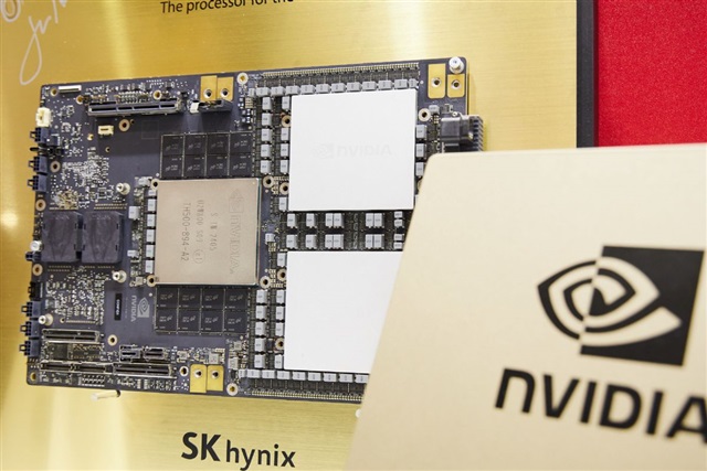
Advanced packaging is moving faster than ever, and the conversation is shifting from strictly wafer-centric techniques to larger, more scalable panel and PCB-based platforms. In that transition, a new approach is stepping into the spotlight: CoWoP, or Chip-on-Wafer-on-Platform PCB. It aims to bring wafer-level precision together with the manufacturing reach, cost structure, and form-factor flexibility of advanced PCB platforms—potentially reshaping how the industry builds AI and high-performance computing systems.
What makes CoWoP compelling
– Hybrid manufacturing flow: CoWoP blends die assembly at the wafer stage with final integration onto a high-density platform PCB. That hybrid flow can open the door to higher throughput and larger build areas than traditional wafer-bound packaging alone.
– Scale for AI era designs: As AI accelerators add more chiplets, memory stacks, and power delivery needs, substrates must carry more signals over shorter distances with tight power integrity. A platform PCB approach provides room for larger interconnect fabrics and integrated power solutions without exploding costs.
– Cost and capacity advantages: Panel and PCB manufacturing can improve economies of scale, making it attractive for ramping volumes while easing pressure on bottlenecked wafer-level capacity.
– Heterogeneous integration: CoWoP is well-suited to mixing logic, memory, and specialty chiplets in one cohesive package, enabling shorter interconnects, higher bandwidth, and better energy efficiency.
Why the industry is looking beyond wafer-only packaging
– Exploding bandwidth and power demands from AI and HPC workloads are pushing existing 2.5D and 3D methods to their limits.
– Capacity constraints and long lead times in some advanced flows are prompting companies to diversify how they integrate chiplets and memory.
– Panel-level and PCB platforms provide a path to larger, more modular designs, with the potential for faster cycle times and lower total cost of ownership.
Key technical hurdles to solve
– Warpage and mechanical stability at panel scale require new materials, stack-ups, and process controls.
– Ultra-fine alignment and die placement accuracy must meet or exceed wafer-level standards to maintain yield and performance.
– Signal and power integrity across large platforms call for careful co-design of interconnect density, decoupling, and thermal paths.
– Reliability over temperature cycles and long service life must be proven for data center and enterprise deployments.
What this means for chipmakers and system builders
– More integration options: CoWoP adds another tool to the packaging toolbox alongside 2.5D, 3D stacking, and advanced substrates. Teams can choose the right mix based on performance targets, cost, and time-to-market.
– Faster design cycles: With platform PCBs offering larger routing real estate, engineers can prototype complex chiplet configurations with fewer compromises.
– Ecosystem shift: Success hinges on tighter collaboration between foundries, OSATs, substrate and PCB vendors, materials suppliers, and EDA providers to co-optimize electrical, mechanical, and thermal performance.
The bottom line
CoWoP crystallizes a broader industry pivot: using the precision of wafer-level assembly where it matters most, then leveraging panel and PCB platforms to scale. For AI accelerators, high-bandwidth memory integration, and dense chiplet designs, that hybrid approach could deliver the bandwidth, power efficiency, and manufacturing headroom the market urgently needs—while setting the stage for the next wave of heterogeneous computing.