China’s New EUV Light Source Prototype Shows Progress, But Replacing ASML Is Still a Long Road
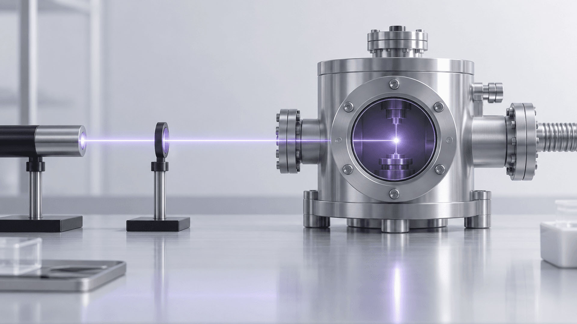
China’s push for homegrown semiconductor manufacturing technology has taken another visible step forward. At the 26th China International Industry Fair in Shanghai, Chinese technology startup Langdao Silex introduced its self-developed EUV light source prototype, called the FlintNano LPP-OXXO.
The announcement quickly drew attention because EUV lithography is one of the most important technologies used in producing advanced chips. Today, ASML remains the dominant supplier of complete EUV lithography machines, making any Chinese progress in this area a major topic for the global semiconductor industry.
Langdao Silex says it has independently developed most of the key components used in its EUV light source, claiming a localization rate of around 90 percent. On paper, that sounds like a significant milestone for China’s chip equipment ambitions. However, while the prototype is an important development, it does not mean China is close to replacing ASML anytime soon.
The FlintNano LPP-OXXO uses laser-produced plasma technology, commonly known as LPP. This method relies on high-power lasers to create plasma, which then generates extreme ultraviolet light. It is the same general approach used in modern EUV lithography systems.
According to the company’s disclosed specifications, the system has a driving laser output of 1,000W, a repetition rate ranging from 1kHz to 20kHz, and a conversion efficiency of more than 2 percent. The EUV output is said to be 15W or higher, with the ability to operate continuously for over 100 hours.
Other technical figures include a plasma size of 60μm, plasma stability of 3 percent RMS, and energy stability of roughly 5 percent. Langdao Silex representatives say the prototype is currently suitable for wafer exposure testing, which is an important early-stage step in EUV lithography development.
Still, wafer exposure testing and mass production are very different challenges.
Building a prototype EUV light source is only one part of the equation. Commercial chip production requires extreme reliability, repeatability, precision, and uptime. In advanced semiconductor manufacturing, even minor instability can affect yield, cost, and production efficiency. That is where the gap between a promising prototype and a fully commercial EUV lithography system becomes much larger.
Langdao Silex estimates that large-scale commercial production could take another three to five years. That timeline may be possible under ideal conditions, but it also appears optimistic. Developing the light source is only one piece of a much larger and more complex machine.
A complete EUV lithography system also requires ultra-precision optics, advanced wafer stages, high-performance control systems, contamination management, vacuum technology, metrology, software integration, and countless other subsystems working together with extreme accuracy.
ASML’s EUV machines are known for their complexity, with hundreds of thousands of components sourced through a vast global supply chain. The company’s success is not based on one component alone, but on decades of engineering, supplier coordination, manufacturing experience, and field-proven reliability.
That is why China’s EUV progress should be viewed as meaningful but not yet disruptive. A localized EUV light source suggests that Chinese companies are moving in the right direction, especially as the country tries to reduce dependence on foreign semiconductor equipment. However, turning this progress into a complete EUV lithography tool capable of competing with ASML will likely take far longer than a few years.
Some earlier expectations suggested that China could begin trial work on EUV-related equipment as soon as 2025. Even if that happens, trial production does not guarantee commercial readiness. China’s current deep ultraviolet lithography equipment still trails the most advanced foreign systems, and EUV technology is significantly harder to master.
For that reason, a more realistic timeline for competitive domestic EUV systems could stretch closer to eight to ten years, assuming steady progress and no major technical setbacks. Some industry leaders have suggested it could take China as long as 15 years to fully catch up in the most advanced lithography technologies.
Meanwhile, ASML’s more immediate concern may not be China’s prototype progress, but geopolitical pressure. U.S.-led trade restrictions have already limited China’s access to advanced chipmaking equipment, and any further restrictions on DUV lithography tools could affect ASML’s business. China represents a major revenue source for the company, with sales to the region accounting for a substantial share of its annual income.
Ironically, tighter restrictions could also accelerate China’s determination to develop domestic alternatives. If access to foreign equipment continues to shrink, Chinese firms may pour even more resources into EUV light sources, lithography tools, optics, and semiconductor manufacturing infrastructure.
For now, Langdao Silex’s FlintNano LPP-OXXO is an important symbol of China’s growing semiconductor ambitions. It shows that Chinese companies are making progress in one of the toughest areas of chip manufacturing technology. But it is not a sign that ASML’s leadership is under immediate threat.
The road from a working EUV light source prototype to a production-ready EUV lithography machine is long, expensive, and technically unforgiving. China has taken a step forward, but the race to build a true ASML alternative is far from over.


