ASML is preparing a major push to help chipmakers produce far more semiconductors without having to build brand-new cleanroom space. As global demand keeps climbing—fueled by everything from everyday electronics to enterprise computing and AI—leading foundries have been under heavy supply pressure. While the industry’s long-term answer includes expanding factory capacity, ASML appears to have uncovered a faster lever: dramatically increasing the power of the EUV lithography light source at the heart of advanced chip production.
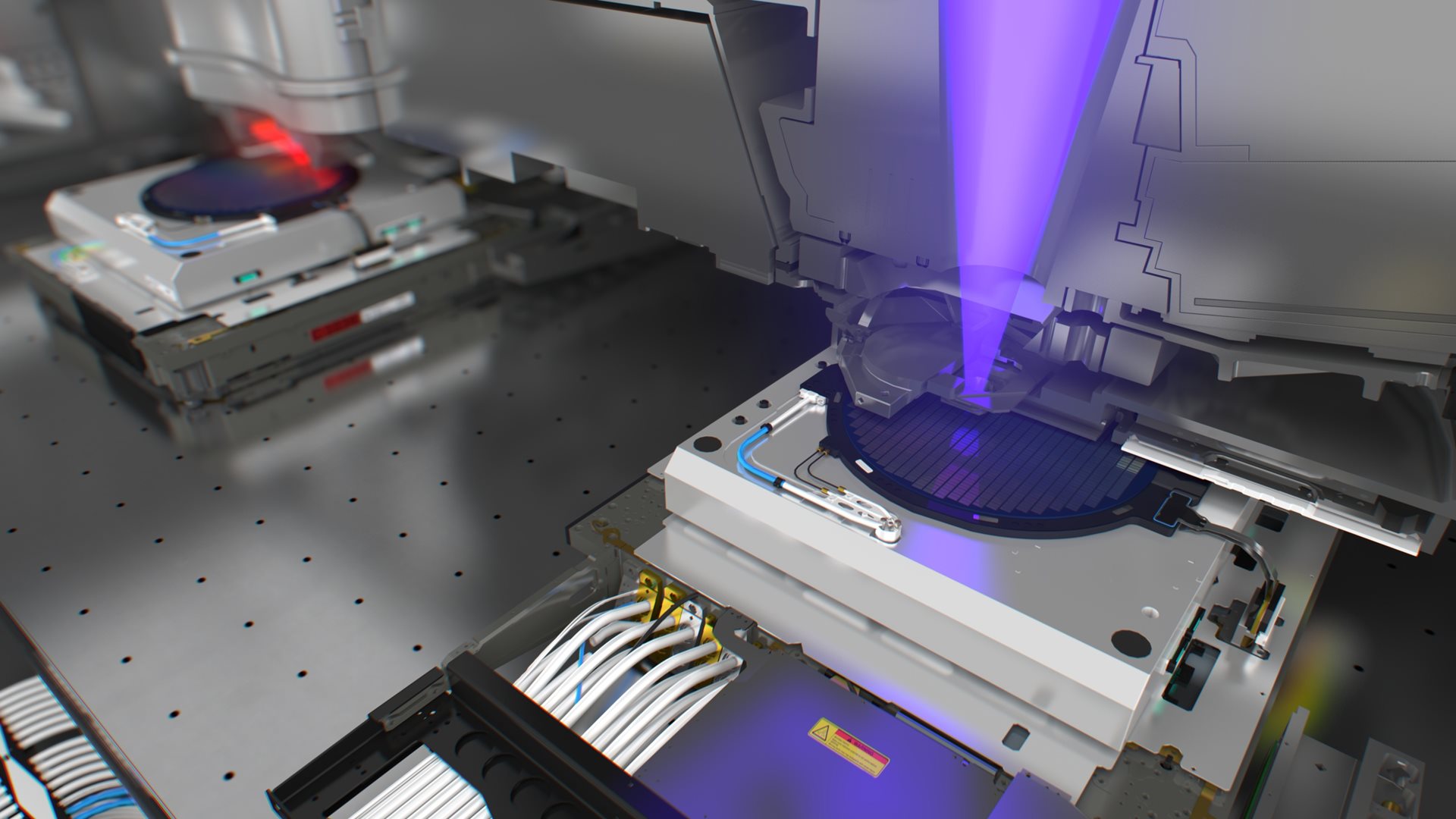
According to a report cited by Reuters, ASML has developed a way to boost EUV light-source power from around 600 watts to 1,000 watts (one kilowatt). The company says this isn’t a brief lab demonstration, but a system designed to operate at 1,000 watts under the same practical, customer-ready requirements expected in real manufacturing environments.
Why does this matter? Because higher EUV source power can translate directly into higher throughput. The expectation is that wafer output could rise from roughly 220 silicon wafers per hour to about 330 wafers per hour—an increase of around 50%—while maintaining similar costs per wafer. If achieved broadly, that kind of jump could significantly ease production bottlenecks across the semiconductor supply chain, especially for advanced nodes where EUV tools are essential.
Just as important is how this improvement might roll out. ASML already offers upgrade paths that allow customers to enhance tool performance without replacing entire systems in the field, using what it calls Productivity Enhancement Packages (PEPs). However, not all older EUV machines can necessarily take full advantage of the 1,000-watt approach due to thermal limitations. Reports suggest the upgrade strategy is more likely to focus on newer EUV platforms such as NXE:3800E configurations, along with the next generation of High-NA systems like the EXE:5000 and EXE:5200.
Beyond boosting output, ASML’s move also reinforces its competitive position in high-end lithography at a time when the geopolitical and competitive landscape is shifting. The report notes that competition pressures—particularly involving China—are part of the broader backdrop, and it also points to emerging challengers working on alternative advanced lithography concepts, including approaches that use shorter-wavelength X-rays generated by particle accelerators.
Even with the excitement, a higher-powered EUV source can bring real engineering challenges for fabs. More power can mean heavier demands on electricity, cooling capacity, and hydrogen flow management. Still, given how intense today’s chip supply constraints remain, manufacturers are likely to view a proven path to 50% more throughput as a potentially game-changing development—one that could reshape fab economics and speed up the pace of chip availability without waiting years for new factories to come online.