China’s semiconductor industry may be on the verge of a major turning point. A new report claims the country has built its first homegrown EUV lithography prototype, a milestone that could eventually reshape China’s ability to manufacture advanced chips without relying on foreign equipment.
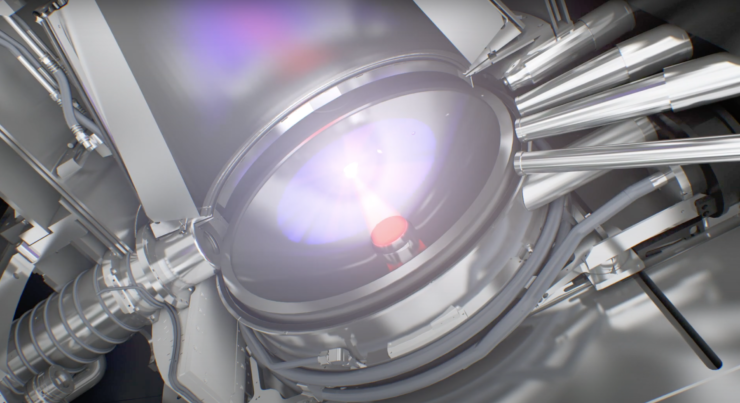
According to the report, the prototype is already operational and can generate ultraviolet light intended for wafer etching, a key requirement for extreme ultraviolet (EUV) lithography. If accurate, this would mark a significant step forward in China’s long-running push to close the gap with the world’s leading chipmaking nations and reduce its dependence on overseas supply chains.
What makes this development especially notable is the speed at which it appears to have progressed. Earlier this year, ASML CEO Christophe Fouquet suggested China would need “many, many years” to develop EUV capabilities. The reported emergence of a working prototype implies China could be closer to semiconductor self-sufficiency than many analysts expected.
That said, there are important caveats. The report indicates Chinese engineers have relied on components sourced from older ASML lithography systems while assembling the prototype. And despite being described as functional, the machine reportedly has not yet taped out an actual chip. In other words, it may be producing light and running in a way that resembles EUV operation, but it hasn’t proven it can deliver real, production-quality results in chip fabrication.
Even with those limitations, sources cited in the report suggest China could make EUV chipmaking more mainstream domestically by 2030. If that timeline holds, it would be far earlier than many past estimates of when China might reach a comparable level of capability in the high-end semiconductor race.
The broader context is hard to ignore: demand for advanced chips inside China has surged, driven in large part by the rapid growth of AI. The pressure to secure local chip capacity has pushed major players to expand manufacturing partnerships and build out new facilities. Huawei, for example, has been closely linked to efforts to strengthen domestic production, and China’s drive for cutting-edge process technology has become more visible in recent years as companies work around restrictions and technical barriers.
This urgency has also shown up in process development. SMIC’s reported N+3 process has been described as a competitor to more mainstream 5nm-class technologies, reflecting how Chinese firms are pushing forward even when access to the most advanced tools is limited.
For now, the biggest unanswered questions are technical. EUV systems are among the most complex machines ever built, and details remain unclear about how this prototype generates its light source, how stable it is, and whether it can meet the precision, yield, and reliability requirements needed for real-world chip production.
Still, if the reported progress is confirmed and continues at pace, China’s EUV prototype could represent one of the most consequential developments in the global semiconductor landscape in years—especially as the battle for AI chips and advanced manufacturing capacity only intensifies.