Creating smaller, more efficient semiconductor chips has been a race for technological supremacy, and nations worldwide are heavily invested in advancing their chipmaking capabilities. One such country is Russia, which is reportedly on its way to producing chips featuring a 350nm process using domestically developed EUV lithography machines, as mentioned by the Deputy Minister of Industry and Trade of the Russian Federation, Vasily Shpak, as reported by Chinese media specializing in semiconductor news.
The importance of semiconductor chips in modern technology cannot be overstated—they are the heart of everything from smartphones to cars and even the simplest of household gadgets. The push to create more powerful and smaller chips is unending, with companies and countries alike striving to overcome limitations and keep pace with growing demands.
Russia’s entry into the production of 350nm chips signifies a notable advancement for the country’s technological progression, especially within the current geopolitical climate that has seen increased emphasis on self-reliance in critical sectors like chip manufacturing.
Understanding the Basics of Chipmaking:
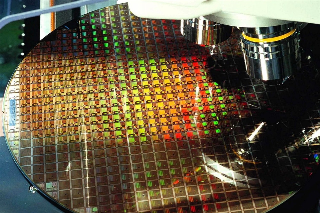
Semiconductor chip manufacturing is an incredibly complex process requiring specialized machinery. One of the key components of this machinery is a photolithography machine, commonly known as a “stepper” or “scanner.” It uses light—extreme ultraviolet (EUV) light, in the most advanced systems—to etch patterns on silicon wafers, which then become the chips. The machine’s ability to use EUV light is critical in permitting the creation of smaller, yet more powerful chips.
Russia’s Development of EUV Lithography Machines:
A major factor in chipmaking is the capacity to develop and build these intricate machines, a feat that traditionally has been dominated by a few key players in the industry. Russia’s announcement that it is not just developing but also expects to produce chips with its self-developed EUV lithography machines is significant and could potentially change the landscape of the semiconductor industry.
Implications and Future Prospects:
The transition to producing 350nm chips is an ambitious one, as the industry standard is quickly moving towards ever-smaller measurements, with 5nm and 7nm processes now being the cutting-edge. However, producing 350nm chips can serve various lesser performance-critical applications and signifies a stepping stone towards more advanced technologies.
Practical Advice and Steps to Consider:
For businesses and technologies reliant on chips, understanding the supply chain, and potential new players, such as Russia, is essential. Staying informed can help prepare for changes in the market.
Identify opportunities where less advanced chips could suffice, potentially reducing costs if these are more readily available or cheaper.
Stay up-to-date with the latest trends and advancements in chip technology to forecast and plan accurately for product development and manufacturing.
By developing its own EUV lithography machines and producing 350nm chips, Russia is joining a critical technological race, one that encompasses not just commercial competition but also touches on national security and economic independence. While the specifications may not meet the most advanced levels currently seen in the semiconductor industry, the potential impact of this development cannot be ignored. It holds relevance for the global chip market and introduces another variable in the intricate equation of global technology supply chains.