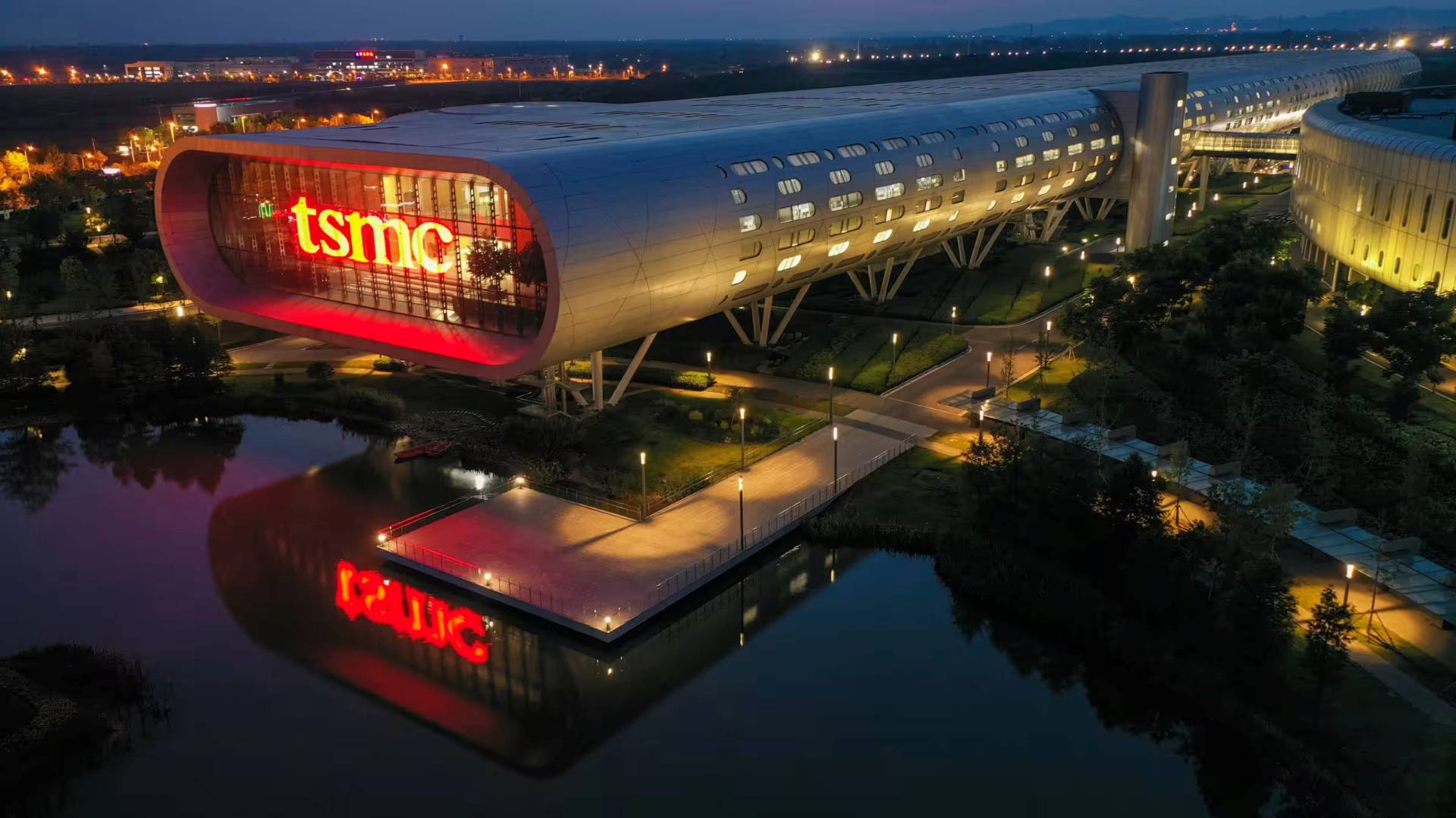
TSMC is laying the groundwork for its next big leap in chipmaking, and all eyes are on the Central Taiwan Science Park. According to a local report, the foundry giant has submitted a land lease briefing that outlines plans to build four plants dedicated to 1.4nm (A14) production. While full-scale output isn’t expected until the second half of 2028, the build-out positions Taiwan at the heart of the next generation of semiconductor manufacturing and is set to create thousands of high-skilled jobs.
The scale is enormous. The initial investment is pegged at around NT$1.5 trillion, roughly $49 billion, to construct the four facilities. Once complete, the project is expected to generate between 8,000 and 10,000 jobs, underlining its significance for the local economy and the global chip supply chain. Early risk production at one of the plants is targeted for late 2027, with mass production slated for late 2028—timelines that align with the industry’s push toward sub-2nm technologies.
Despite the eye-watering capital outlay, the potential payoff is just as striking. Estimated revenue from a single A14 fab could exceed NT$500 billion, about $16.26 billion. With all four plants running at full tilt, annual revenue could approach $65 billion. Those numbers reflect both the complexity and the premium nature of cutting-edge nodes: each 1.4nm wafer could cost around $45,000, making it one of the priciest process technologies ever brought to market.
One of the more surprising elements is the equipment strategy. The report indicates that TSMC does not plan to use its initial investment to purchase next-generation High-NA EUV tools, which can cost roughly $400 million each. Instead, the company aims to reach 1.4nm yields with existing EUV infrastructure, enhanced by photomask pellicles and other process optimizations—an approach that could help rein in costs and accelerate ramp-up.
On the customer front, Apple is widely expected to be among the first to tap A14 capacity. The iPhone maker has a track record of locking down leading-edge supply and is already said to have secured more than half of TSMC’s initial 2nm allocation. Meanwhile, a separate report suggests NVIDIA is currently the only confirmed client for the A16 (1.6nm) process node. If history is any guide, Apple’s early move to pre-order 1.4nm wafers would not be a surprise.
If these timelines hold, the Central Taiwan Science Park will become a focal point for the most advanced silicon on the planet by 2028. The combination of four high-volume 1.4nm fabs, a massive job influx, and a measured equipment strategy underscores TSMC’s intent to maintain process leadership while managing costs and risk. It’s an ambitious bet on the future of compute, AI, and mobile performance—one that could reshape the semiconductor landscape for years to come.
 and A12 (1.2nm) for 2029, Holding Off on ASML’s Most Expensive EUV Machines—for Now")


