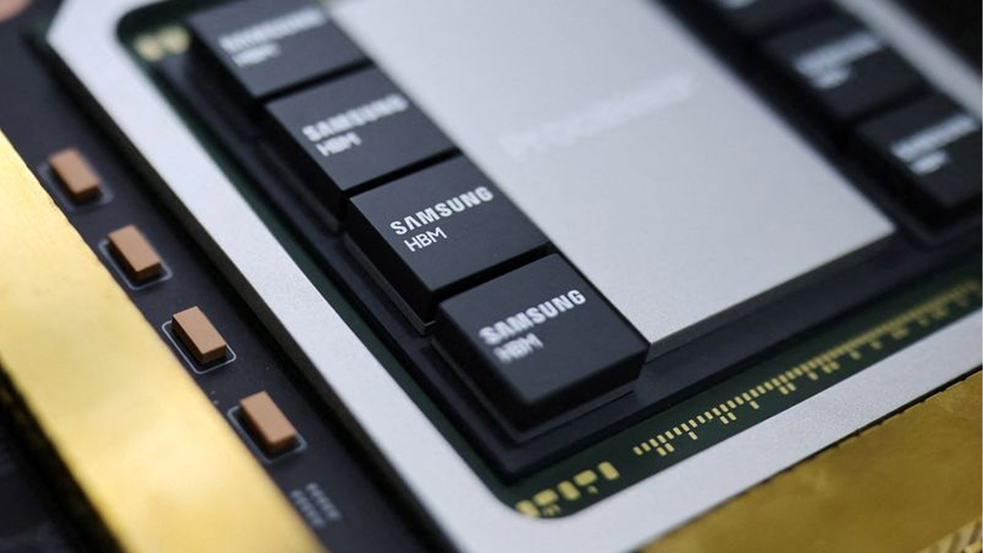
Samsung is reportedly working on a major memory upgrade that could bring High-Bandwidth Memory, better known as HBM, to smartphones and tablets. Until now, HBM has mainly been associated with data centers, AI accelerators, and high-performance computing systems. But with mobile AI becoming a bigger focus, Samsung appears to be preparing a version of the technology designed specifically for compact, power-sensitive devices.
The goal is clear: make future smartphones and tablets faster, more efficient, and better equipped for on-device artificial intelligence. As AI features become more demanding, mobile devices need memory that can move huge amounts of data quickly without draining the battery or producing excessive heat. HBM could help solve that problem, but bringing it to mobile hardware is not simple.
Current mobile DRAM typically relies on copper wire bonding. This design works well for today’s smartphones, but it has limits. The number of I/O terminals usually falls in the 128 to 256 range, which can restrict bandwidth and increase signal loss when manufacturers try to push performance higher. For AI workloads, gaming, image processing, and advanced multitasking, that limitation becomes increasingly noticeable.
Samsung’s reported solution involves a more advanced packaging approach using ultra-high aspect ratio copper pillars combined with Fan-Out Wafer Level Packaging, or FOWLP. This packaging method is already being used to improve heat resistance and sustained performance in advanced mobile processors. By applying it to mobile HBM, Samsung could create memory chips that deliver much higher bandwidth while still fitting inside the tight space available in phones and tablets.
A key part of the development is Samsung’s Vertical Copper Post Stack technology, known as VCS. This method stacks DRAM dies in a staircase-like structure and fills the gaps with copper pillars. The design is intended to help HBM operate efficiently inside thin mobile devices, where size, heat, and power consumption are major challenges.
Samsung has reportedly increased the aspect ratio of these copper pillars from the current 3:1 to 5:1 range to around 15:1 to 20:1. That change could significantly improve memory bandwidth. However, it also creates a new engineering challenge. As the copper pillars become taller and thinner, their diameter may shrink below 10 micrometers. At that scale, the pillars can become fragile, bend, or even break.
That is where FOWLP becomes important. By extending copper wiring outward, the packaging can improve structural strength and reliability. It can also increase the number of I/O terminals, helping deliver an estimated bandwidth improvement of around 30 percent. For future mobile AI chips, that kind of gain could be extremely valuable.
If Samsung succeeds, mobile HBM could become a major leap forward for next-generation smartphones and tablets. Faster memory would help devices process AI tasks locally instead of relying heavily on cloud servers. This could improve response times, privacy, image generation, voice recognition, real-time translation, camera processing, and productivity features.
However, the technology is still in development, so it is unclear when consumers will see it in commercial devices. One possibility is that Samsung could introduce mobile HBM in a future Exynos processor, potentially around the Exynos 2800 or Exynos 2900 generation. The Exynos 2800 has also been rumored to include Samsung’s first in-house GPU, which would make faster memory even more useful for graphics and AI performance.
Samsung may not be the only company interested in bringing HBM to mobile devices. Apple has also been rumored to be exploring HBM for future iPhones, although it remains uncertain whether Samsung would supply the technology. Huawei is reportedly studying similar possibilities as well, though Samsung entering that company’s supply chain appears unlikely.
Despite the promise, cost could slow adoption. Mobile DRAM prices have already become expensive, and HBM is typically far more costly than standard memory. Smartphone brands may hesitate to use it until pricing becomes more reasonable. If memory costs remain high over the next few years, companies may continue improving on-device AI mainly through faster chipsets, upgraded neural processing units, and better storage technology rather than HBM.
Still, Samsung’s work suggests that the future of mobile memory could be changing. As AI becomes one of the biggest selling points for premium smartphones and tablets, faster and more efficient memory will be essential. Mobile HBM may not arrive immediately, but it could eventually become a key feature in flagship devices built for advanced artificial intelligence, high-end gaming, and professional workloads.