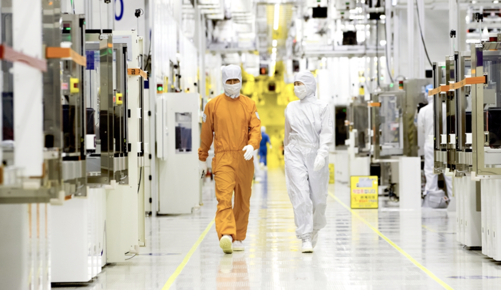
Samsung is reportedly seeing a surge of interest in its 4-nanometer chip manufacturing process, as customers line up for production capacity that may already be booked out well into 2027. New information from Korean industry sources suggests that Samsung Foundry’s 4nm node is benefiting from improving stability and strong demand tied closely to the booming AI and memory ecosystem.
The 4-nanometer technology, commonly known as SF4, entered mass production in 2021 and has since evolved through multiple refinements. Over time, Samsung has introduced several variants designed to meet different performance and efficiency targets, including SF4E, SF4P, SF4X, and SF4A. The latest generation, SF4X, is widely described as being optimized for high performance computing needs and enhanced by more advanced back-end processing techniques—an important detail as chipmakers compete to deliver better speed, power efficiency, and manufacturing consistency.
One key reason behind the renewed momentum is reportedly stronger-than-expected stability. A source cited by Korean press indicates that reliability improvements have encouraged additional orders from global customers. The same source claims the squeeze isn’t limited to a short window—manufacturing lines are said to be heavily loaded, leaving capacity tight not only through next year but potentially far beyond, due to packed production schedules.
At the same time, rising demand for next-generation high-bandwidth memory is believed to be adding pressure to Samsung’s manufacturing capacity. HBM4 in particular is emerging as a major driver as AI accelerators and data center workloads grow. Samsung announced earlier this year that it shipped its first commercial HBM4 products to customers and began mass production. In this memory design, the logic die is reportedly produced using Samsung’s 4-nanometer process, while other parts of the memory stack are made using a separate 1c process technology. Industry competition is also intensifying, with rivals showcasing advanced high-stack HBM4 packages aimed at the same AI-driven market.
Recent chatter about manufacturing performance has also helped boost confidence in Samsung’s 4nm node. A prior report suggested yields may have reached around 80%, and multiple major technology companies are rumored to be evaluating or placing orders. In the latest round of claims, NVIDIA is mentioned again, and Google is also described as having interest in Samsung’s 4-nanometer manufacturing capabilities—an attention signal that matters because large-scale customers typically seek proven yield, stable output, and predictable long-term capacity.
If the order pipeline holds, it could translate into a meaningful financial turning point for Samsung Foundry. The report suggests the foundry business could potentially move into profitability as early as the second half of this year, supported by stronger utilization and higher-volume commitments.
However, there’s still uncertainty around where exactly these new orders would be manufactured. It remains unclear whether production would be routed primarily through Samsung’s facilities in Korea or through the company’s U.S. expansion in Taylor, Texas. That question matters because the cost structure and accounting treatment of major facility buildouts can significantly influence when and how profitability shows up on the books. In other words, even if demand is strong, the financial outcome may depend on how startup and construction costs are ultimately handled.
Overall, the latest reporting paints a picture of Samsung’s 4nm process entering a more confident phase—supported by iterative improvements, demand from AI and high-performance computing, and a memory market increasingly centered on advanced HBM4. If these trends continue, Samsung Foundry’s SF4 family could remain in heavy demand for years, especially as data center customers push for faster, more efficient compute and memory platforms.