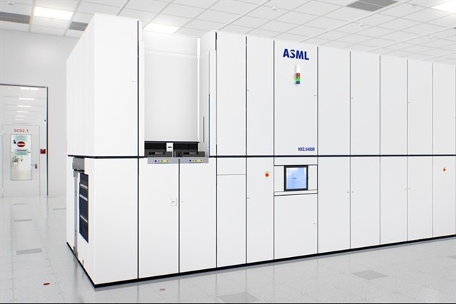
Samsung Electronics is gearing up to make a significant leap forward in the semiconductor industry with the introduction of its first High-NA EUV (extreme ultraviolet lithography) equipment, anticipated for early 2025. This move is set to solidify the company’s standing as a powerhouse in advanced semiconductor production.
Harnessing High-NA EUV technology means Samsung will be able to produce chips with even more precise details and increased efficiency. This cutting-edge equipment allows for the creation of smaller, more powerful semiconductors, which are crucial for supporting the growing demands of modern technology, from smartphones to data centers.
The integration of this technology marks a pivotal moment not just for Samsung, but for the entire tech industry. As the global market continuously pushes towards miniaturization and higher performance, Samsung’s advancements could lead to substantial improvements in the performance of a multitude of electronic devices.
With this step, Samsung may not only enhance its competitive edge but could also influence industry-wide standards in semiconductor manufacturing. As the launch draws nearer, eyes will be on the South Korean giant to see how this innovative technology will impact the future of electronics. This major progression is expected to usher in a new era of possibilities in the technology landscape, promising exciting developments ahead.