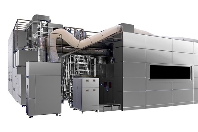
Nikon is setting its sights on a significant innovation in the semiconductor industry. The company has revealed its intention to introduce a groundbreaking piece of technology by the fiscal year 2026. This new project will focus on offering exposure equipment specifically designed for the back-end semiconductor process. What makes this initiative particularly intriguing is Nikon’s commitment to employing a photomask-free approach, marking a bold new direction in the company’s technological endeavors.
This development signifies Nikon’s inaugural foray into the realm of back-end semiconductor exposure equipment, a venture that holds the promise of reshaping industry standards. By eliminating the need for photomasks, Nikon aims to streamline the semiconductor manufacturing process, potentially reducing production time and costs, while also enhancing efficiency.
Nikon’s strategic move into this arena reflects its dedication to innovation and its desire to address the evolving needs of the semiconductor market. As the company gears up for this ambitious project, it positions itself as a forward-thinking leader in the adoption of advanced technological solutions.
The anticipation builds as industry insiders and tech enthusiasts await further details on how Nikon plans to bring this photomask-free technology to fruition, and the potential impact it may have on the semiconductor industry at large. With this announcement, Nikon promises a future where semiconductor manufacturing could become more accessible and efficient, paving the way for technological advancements and industry growth.