Chinese engineers reportedly tried to reverse-engineer an ASML deep ultraviolet (DUV) lithography machine—and ended up breaking it. According to accounts circulating in industry circles, the team disassembled an older system in hopes of understanding its inner workings, but the machine failed after reassembly. When they asked ASML for help, visiting technicians allegedly discovered the damage was caused by a reverse-engineering attempt rather than a routine malfunction. The claim has not been verified by ASML.
The story highlights the intense pressure inside China’s semiconductor sector. With limited access to cutting-edge lithography tools, domestic chipmakers have struggled to scale production and improve yields. Companies such as SMIC have pushed forward, but without sufficient availability of advanced lithography equipment, output and process migrations remain constrained.
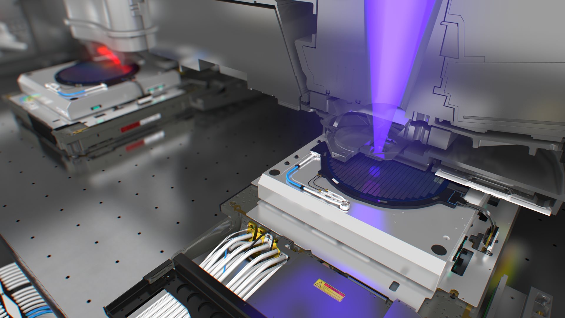
Why would anyone risk cracking open a DUV scanner? Because modern chipmaking lives or dies by lithography. These systems are the beating heart of a fab, defining pattern fidelity, throughput, and ultimately cost per wafer. But they’re also among the most complex machines ever built. A single DUV tool integrates ultra-precise optics, vibration-damped stages that move with nanometer accuracy, powerful lasers, vacuum chambers, and labyrinthine control software. Even a speck of contamination or a slight misalignment can throw off performance.
Reverse engineering a machine like this is far from straightforward. Beyond the hardware, there are calibration baselines, test routines, and service keys that tie the system to OEM-certified parts and procedures. Many subsystems track their own health and expect specific responses during diagnostics. If those expectations aren’t met—or if third-party parts are used—faults can cascade. Re-establishing factory-grade alignment and cleanliness often requires specialized tooling, proprietary data, and trained field engineers.
China has made real strides in developing homegrown lithography tools, but matching ASML’s performance and reliability remains difficult. The Dutch company has spent decades refining DUV and EUV platforms; its flagship EUV machine is famously massive—roughly the size of a bus—and relies on an intricate supply chain and extreme tolerances that are hard to replicate. That gap explains both the urgency behind domestic R&D and the temptation to learn by taking older systems apart.
If accurate, the reported incident underscores three realities. First, the bottleneck in lithography is still the single biggest brake on China’s semiconductor ambitions. Second, high-end scanners are designed to be serviced by the manufacturer, with deep integration between hardware, software, and certified parts. Third, shortcuts in such a sensitive domain can backfire, potentially damaging irreplaceable equipment and triggering lengthy downtime.
As the global chip race intensifies, expect continued investment in domestic lithography and support ecosystems, from optics and lasers to metrology and contamination control. Progress is happening, but the road to parity with established leaders is long and unforgiving. For now, the tale serves as a reminder: in advanced manufacturing, the hard part isn’t just building the machine—it’s mastering everything that keeps it perfectly calibrated, clean, and repeatable, day after day.