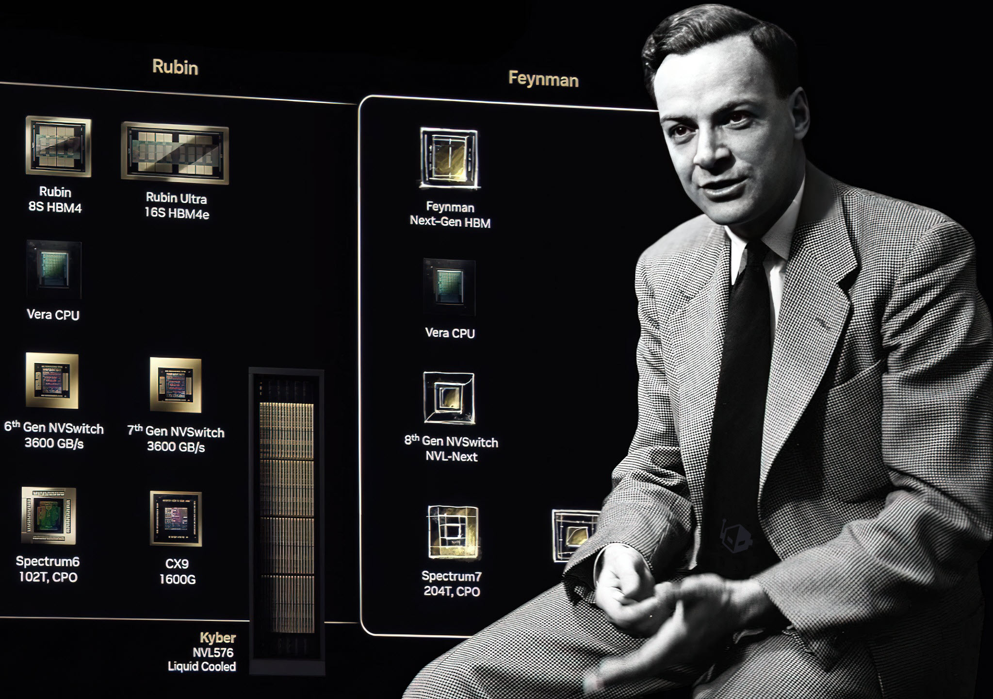
NVIDIA is reportedly lining up a major shift in how it builds future AI hardware, aiming to take tighter control of the inference stack with its next-generation Feynman chips. The big idea: bring LPU-style acceleration into the GPU package itself, potentially using advanced 3D stacking to unlock faster, more efficient inference performance.
A recent analysis from GPU expert AGF suggests NVIDIA could introduce Groq-derived LPU blocks in the Feynman generation, expected around 2028 after Rubin. The promise of these LPU units is especially compelling for inference workloads, where deterministic, compiler-driven dataflow and static low-latency scheduling can raise Model FLOPs Utilization (MFU), particularly in low-batch scenarios that often struggle to keep conventional GPU pipelines fully utilized. In practical terms, this could mean a noticeable jump in real-world inference throughput and responsiveness for deployed AI models.
How would NVIDIA physically integrate LPUs into a future GPU? One proposal gaining attention is 3D stacking using TSMC hybrid bonding, similar in concept to how other high-performance chips have stacked extra cache dies directly on top of compute silicon. Instead of trying to build massive SRAM directly onto an advanced-node GPU die, the theory is that NVIDIA would keep the main Feynman compute die on a cutting-edge process (such as a 1.6nm-class node) for tensor compute, control logic, and core GPU functionality, while stacking separate LPU-focused dies that include large SRAM banks.
This approach targets a key economic and technical problem: SRAM scaling doesn’t improve at the same pace as logic, and putting large amounts of SRAM on the most advanced silicon can be an inefficient use of expensive wafer area. By moving large SRAM banks to a separate die and bonding it directly to the compute die, NVIDIA could reserve the newest process technology for what benefits most from it (dense compute) while still getting extremely fast access to SRAM through a wide, low-energy interface.
Hybrid bonding matters here because it can deliver a much wider connection and lower energy per bit than off-package memory approaches. If the main compute die also uses backside power delivery, that can free up the front side for dense vertical connections to stacked SRAM/LPU dies, helping reduce latency and improving the speed of decode and data movement—areas that are critical for inference efficiency.
Still, stacking LPU dies on top of a high-density compute die introduces serious tradeoffs. Thermals are one of the biggest. Packing multiple active layers together makes heat removal harder, and inference-focused blocks built for sustained throughput could create new hotspots or bottlenecks. Beyond cooling and packaging, there’s also a deeper execution-level challenge: LPUs favor a fixed, deterministic execution order, while GPUs are prized for flexibility and dynamic scheduling. That tension—determinism versus flexibility—could become a defining design constraint if NVIDIA tries to blend both paradigms in one tightly integrated architecture.
There’s also the software elephant in the room. CUDA is built around hardware abstraction and a mature GPU programming model, while an LPU-style approach can require more explicit control over memory placement and execution flow. Even if NVIDIA solves the hardware integration with stacked dies and hybrid bonding, getting CUDA and the broader AI software ecosystem to fully exploit an LPU-GPU hybrid—without forcing developers into painful rewrites—may be the hardest part. Making SRAM-rich, LPU-like execution play nicely inside a GPU-first programming world would require major engineering and tooling advances.
If NVIDIA goes through with it, the payoff could be significant: stronger leadership in AI inference performance, better utilization in low-batch deployment scenarios, and a more vertically optimized inference platform. The cost is complexity—thermal, architectural, and software-level complexity that NVIDIA would need to master to make Feynman a true inference powerhouse.