NVIDIA may turn to Intel’s advanced Foveros chip packaging technology for future AI products, according to a new analyst report from South Korea’s GF Securities. If accurate, the move could mark another important step for Intel’s foundry ambitions while also helping ease pressure on TSMC’s highly demanded advanced packaging capacity.
The latest claim builds on earlier industry speculation that NVIDIA has been evaluating Intel’s next-generation manufacturing and packaging technologies for future GPU designs. While NVIDIA is still expected to rely heavily on TSMC for its most advanced GPU dies, Intel could reportedly play a role in supporting non-core components or backend production needs.
In semiconductor manufacturing, chip production is often split into two major stages: frontend and backend. The frontend stage involves creating the actual chip circuitry on silicon wafers, which determines the processor’s core performance and computing capability. The backend stage takes place after the wafer is processed and includes cutting, assembling, packaging, and preparing the chip for use in finished systems such as AI servers and data centers.
This backend stage has become increasingly important as demand for artificial intelligence hardware continues to surge. Modern AI accelerators are no longer simple single-die chips. They often combine multiple chiplets, memory stacks, interconnects, and specialized components in one advanced package. As a result, packaging technologies are now a critical factor in performance, power efficiency, and production capacity.
Intel has been working to strengthen its position in advanced packaging even as it continues to compete with TSMC in leading-edge chip manufacturing. The company’s existing packaging technologies include EMIB and EMIB-T, which are designed to connect multiple chip components efficiently within a single package. These technologies have attracted attention from major technology companies developing custom AI processors.
Foveros, however, represents a more advanced approach. Unlike traditional packaging methods that place chiplets side by side, Foveros enables true 3D stacking, allowing compute tiles or chiplets to be stacked vertically on top of a base die. This design can reduce the physical footprint of the chip package while improving power delivery, communication speed, and overall efficiency.
For AI accelerators, those improvements can be highly valuable. Data movement between chip components is one of the biggest challenges in high-performance computing. By stacking components more closely together, 3D packaging can help reduce latency and improve bandwidth, both of which are essential for training and running large AI models.
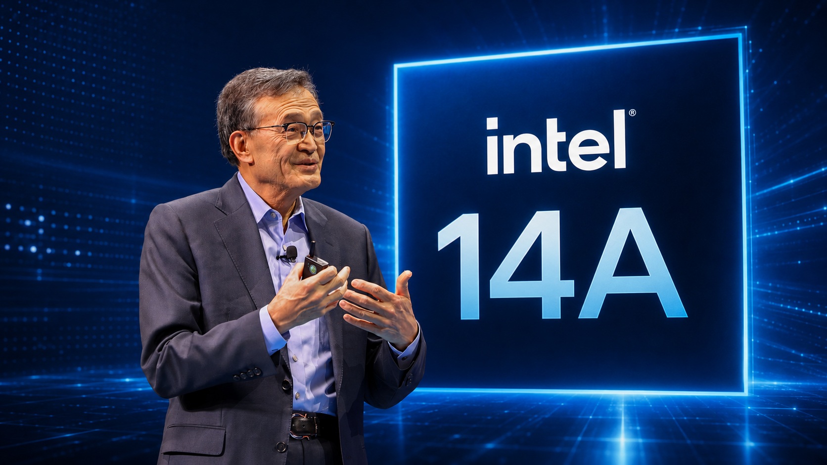
According to analyst Jeff Pu of GF Securities, Intel’s 14A process is expected to move into production in the second half of 2028, and NVIDIA could potentially use Intel’s Foveros packaging technology around that same timeframe. The report does not provide extensive technical details, but it supports previous claims that NVIDIA may be exploring Intel’s technologies for future GPU platforms.
Earlier reports suggested that NVIDIA could consider Intel’s 18A or 14A process technologies for its future Feynman GPU generation. Those claims indicated that TSMC would likely remain responsible for the main GPU die, while Intel could be used for other parts of the design or advanced packaging work.
If NVIDIA does adopt Intel Foveros for future AI chips, the decision could benefit multiple companies across the semiconductor supply chain. NVIDIA would gain access to additional advanced packaging capacity at a time when AI chip demand remains extremely high. Intel would secure a major endorsement for its foundry and packaging business. TSMC, meanwhile, could see some relief from the intense demand placed on its own advanced packaging services.
The global AI boom has created a major bottleneck in semiconductor packaging. High-end AI GPUs require sophisticated integration with high-bandwidth memory and other components, making advanced packaging one of the most constrained parts of the industry. As companies race to build larger AI data centers, access to packaging capacity has become nearly as important as access to leading-edge wafer production.
For Intel, a potential partnership with NVIDIA would be especially significant. The company has invested heavily in becoming a major contract manufacturing and packaging provider, and winning business from one of the world’s most important AI chip designers would strengthen its credibility in the market.
Still, the reported timeline suggests that any NVIDIA use of Intel Foveros technology would not happen immediately. With Intel 14A production expected later in the decade, the potential collaboration appears tied to future AI GPU generations rather than current products.
For now, NVIDIA continues to dominate the AI accelerator market, while TSMC remains its most important manufacturing partner. But as AI hardware becomes more complex and demand keeps rising, NVIDIA may increasingly look to diversify its supply chain and tap additional advanced packaging technologies.
If the latest analyst claims prove accurate, Intel’s Foveros could become part of NVIDIA’s long-term AI chip strategy, signaling a major shift in how future high-performance GPUs are designed, assembled, and scaled for the data center market.