Intel’s foundry push is picking up momentum, and new supply-chain chatter suggests some of the biggest names in tech are paying close attention. With demand for CPUs and AI silicon surging thanks to the agentic AI and inference boom, chipmakers across the industry are running into tight capacity. That backdrop is creating an opening for Intel Foundry to win business with its next-generation manufacturing nodes and advanced packaging options.
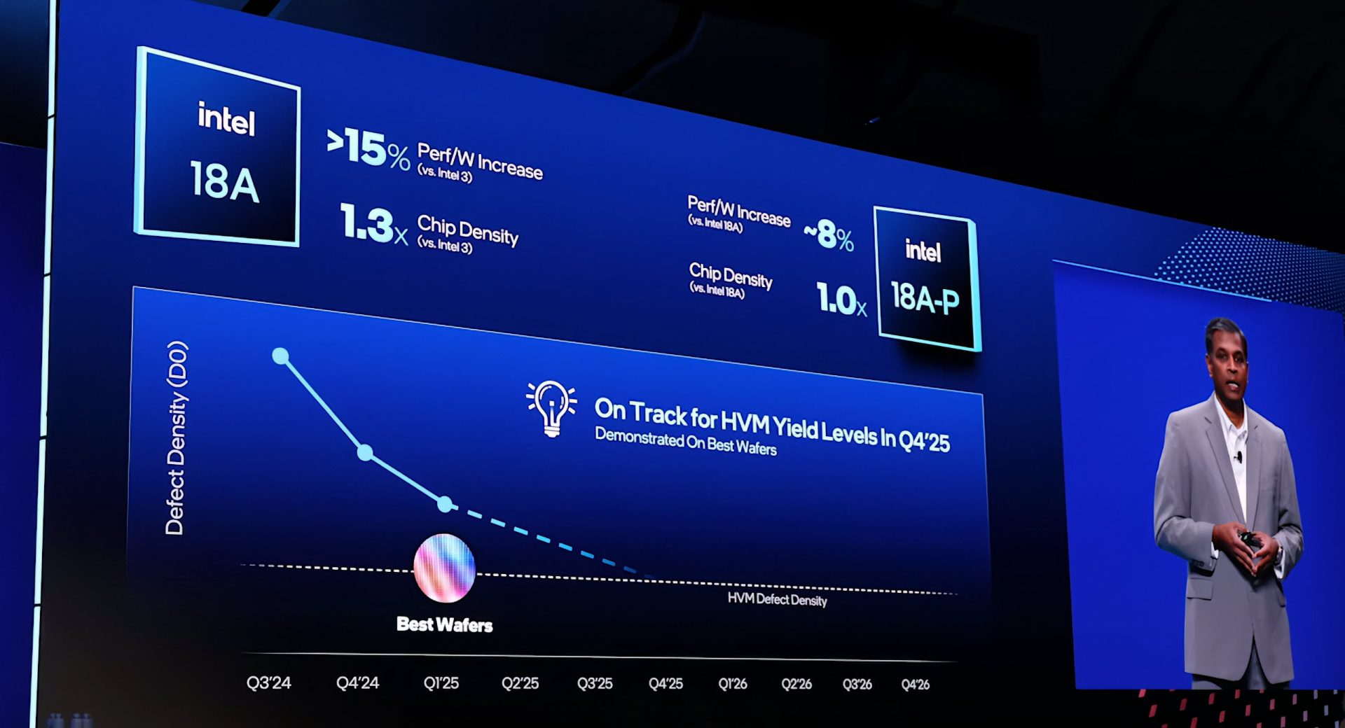
According to supply-chain sources, multiple customers have already started test chip verification using Intel’s 18A process. That’s a meaningful step, because test silicon is one of the clearest signs a manufacturing technology is moving from promise to practical readiness. These efforts also appear to be progressing in parallel with Intel’s 18A-P rollout, which is positioned as an enhanced version of 18A.
One factor helping adoption is the continued maturation of Intel’s process design kit (PDK), the essential toolset chip designers rely on to build and validate designs for a specific manufacturing node. As the 18A PDK becomes more robust, customer confidence and participation reportedly increase. On top of that, Intel’s 14A node is also advancing, with PDK 0.9 expected by the end of the year—another signal that Intel wants to keep a steady cadence of foundry deliverables.
18A-P is expected to bring a notable efficiency uplift. Intel’s messaging puts 18A-P at around an 8% improvement in performance per watt compared to 18A, while maintaining the same density levels. In a market where power efficiency increasingly decides everything from laptop battery life to data center operating costs, performance-per-watt gains like that can be a decisive selling point.
The same supply-chain reporting claims Apple is among the high-profile customers expected to use Intel Foundry, potentially tapping 18A-P for future “M” series chips aimed at client devices. Meanwhile, Google is said to be interested in Intel’s EMIB advanced packaging technology for an upcoming TPUv8e AI accelerator. EMIB, Intel’s embedded multi-die interconnect bridge approach, is designed to connect multiple pieces of silicon inside a single package with high bandwidth and efficiency—an area where advanced packaging has become just as strategic as the process node itself.
Intel hasn’t publicly confirmed major customer wins beyond previously mentioned partnerships, but the broader picture is that its foundry roadmap is drawing serious external attention. That aligns with Intel’s recent statements that it has already achieved high-volume manufacturing readiness for 18A with Panther Lake. If Panther Lake ramps as expected and expands across retail and mainstream PC segments, it could serve as both a revenue driver and a proof point for Intel’s 18A family in real-world products.
Looking ahead, more clarity may arrive as Intel continues to outline its foundry strategy and technical milestones over the coming year. With AI-driven compute demand still climbing and supply constraints pressuring the industry, Intel’s 18A-P, 14A, and EMIB packaging offerings are increasingly positioned as key pieces of the company’s plan to compete for next-generation silicon from major customers.