Intel appears to be on the verge of a groundbreaking moment with its 18A process, drawing significant interest from major tech companies. This development could mark a pivotal breakthrough for Intel’s Foundry Division, as they seek to shift attention away from TSMC, especially in the U.S. market.
Intel’s chip business is eager for success both financially and in reputation, aiming to rival TSMC’s dominance following its strong ties with the U.S. government. As companies view TSMC’s U.S. facilities as a solid choice, Intel’s 18A node emerges as a promising alternative. According to a report, Intel is in discussions with industry leaders like NVIDIA, Microsoft, and Google about the potential of this innovative process, which could stand toe-to-toe with TSMC’s N2 node.
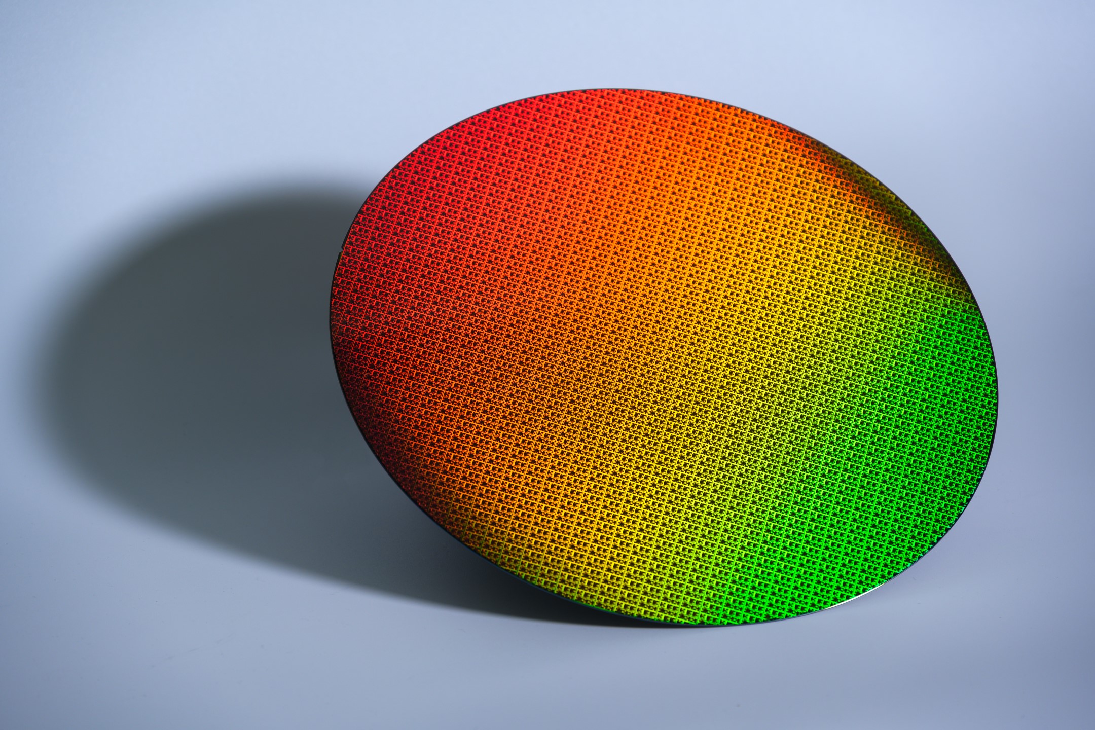
During the recent Direct Connect 2025 event, Intel highlighted the advantages of the 18A node, claiming it as the “most advanced process manufactured in the U.S.” With comparable SRAM density and performance metrics to TSMC’s N2, the 18A node is expected to significantly surpass Intel’s previous generation processes, capturing the interest and excitement of potential clients.
The surge in interest is partially attributed to new leadership under CEO Lip-Bu Tan, who is steering Intel towards advancements in semiconductor design automation, packaging, and foundry operations. With a potential shift from the “IDM 2.0” strategy, Intel might also enhance its presence in the consumer market, particularly in CPUs.
Additionally, TSMC’s production lines are currently overwhelmed, prompting firms to seek alternatives. Intel, therefore, stands ready to compete as a viable counterpart to TSMC’s 2nm node, although competitors like Samsung Foundry are also vying for position. Intel’s strategic moves with the 18A process could redefine its role and impact in the semiconductor industry.