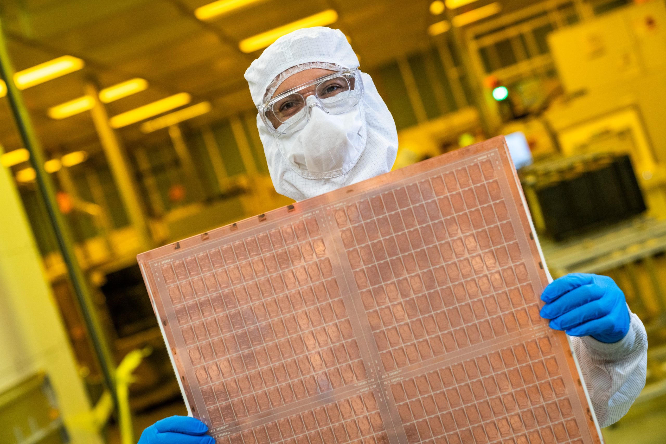
Intel is pressing ahead with its glass substrate program, pushing back on rumors that it has either fast-tracked commercialization or abandoned the effort altogether. The company says its development timeline remains aligned with the roadmap it outlined last year, and it is not licensing the technology to Samsung at this time.
Glass substrates are emerging as a critical piece of advanced semiconductor packaging, offering a path beyond traditional organic materials. By switching to glass, chipmakers can target higher reliability and finer interconnect density thanks to glass’s exceptional flatness and thinness. The result can be stronger packages built to handle the complexities of high-performance computing, AI accelerators, and next-gen chiplet-based designs.
Benefits often cited for glass substrates include:
– Higher mechanical strength for improved durability and reliability
– Potential for greater interconnect density due to thinner, flatter layers
– Better dimensional stability that supports advanced routing at tight tolerances
Recent industry chatter suggested Intel’s momentum had slowed, fueled in part by reports that key contributors to its glass effort had left for roles at a major competitor’s components division. That spurred speculation about both a possible exit from the program and a stopgap licensing deal to mitigate the cost of new manufacturing investments. Intel’s latest stance aims to clear that up: the plan hasn’t changed, and there’s no licensing deal in place.
This clarity matters. Advanced packaging has become a decisive battleground as the industry pushes performance without relying solely on shrinking transistors. Glass substrates are viewed as a promising path to scale interconnects, boost power and signal integrity, and support larger, more complex multi-die assemblies.
While the company continues to navigate a challenging market environment, staying the course on glass substrates signals a long-term bet on foundational packaging innovation. If executed well, it could give future Intel platforms a meaningful edge in density, reliability, and high-performance computing capabilities—areas that will define the next wave of semiconductor leadership.