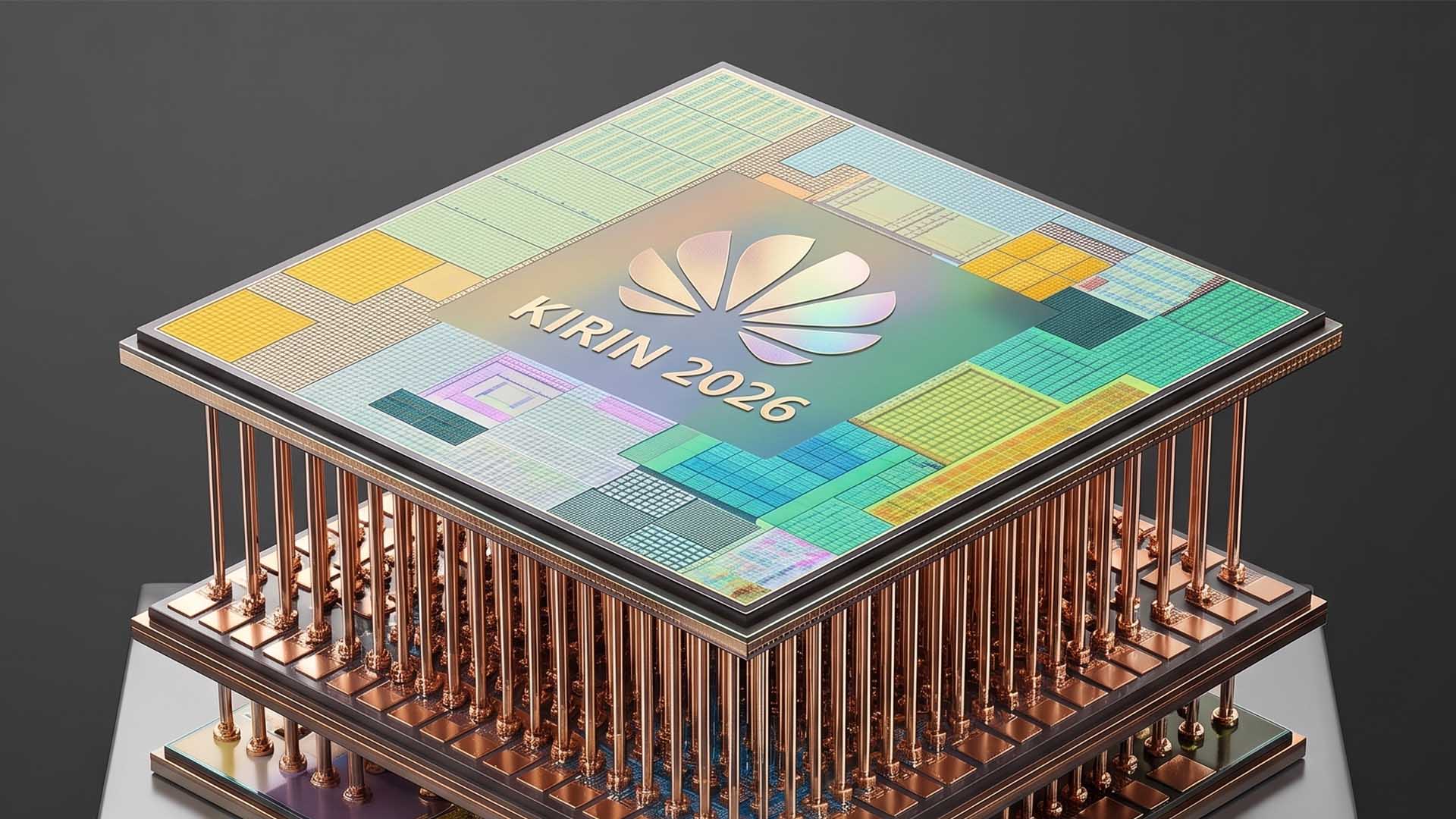
Huawei’s Kirin 2026 could become one of the company’s most important mobile chipsets yet, not because it relies on the world’s most advanced lithography, but because it may use smarter packaging to work around that limitation.
With restricted access to cutting-edge EUV chipmaking tools, Huawei has been forced to find alternative ways to improve smartphone processor performance. Instead of depending solely on smaller manufacturing nodes, the company is focusing on advanced chip packaging, and its proposed hybrid bonding technology could play a major role in the future of Kirin chips.
Huawei has outlined a 3D chip stacking approach that could allow different parts of a system-on-chip to be placed vertically rather than spread out across a traditional flat design. This method, shown as part of Huawei’s LogicFolding Design concept, is intended to increase transistor density, improve efficiency, and shorten communication paths between key components.
In a conventional mobile chipset, parts such as the CPU, GPU, NPU, memory, and other logic blocks communicate across relatively longer distances. With 3D stacking, those distances can be reduced dramatically. Instead of data traveling across millimeters, it may only need to move across micrometers. That kind of reduction can lead to faster communication, lower latency, and better power efficiency.
The potential benefits are especially important for next-generation smartphones. Mobile processors are increasingly expected to handle demanding workloads such as gaming, computational photography, and on-device AI processing. These tasks require high bandwidth between different chip components, and they also place heavy pressure on power consumption and heat management.
Hybrid bonding could help address these challenges. By creating dense vertical interconnects between stacked layers, Huawei could improve bandwidth while reducing the energy needed to move signals across the chip. In simple terms, the chip may be able to do more work while wasting less power.
This is particularly relevant because Huawei is believed to be relying on SMIC’s 7nm-class manufacturing process for advanced chip production. While that process is not as advanced as the latest nodes used by leading global foundries, advanced packaging could help narrow the performance and efficiency gap. Instead of shrinking transistors further, Huawei appears to be exploring how to arrange and connect them more intelligently.
The Kirin 2026 is expected to showcase this direction. If Huawei can successfully bring hybrid bonding and 3D stacking into mass production, it could give the company a stronger position in the competitive smartphone processor market, despite the ongoing restrictions it faces.
Huawei is not alone in rethinking mobile chip packaging. Across the industry, chip designers are moving beyond older Package-on-Package methods because traditional layouts can limit peak performance and create thermal challenges. Separating memory from the main silicon die, improving direct heat transfer, and using larger cooling surfaces are all becoming more important as mobile processors grow more powerful.
Samsung is also expected to explore new thermal and packaging strategies for future Exynos chips, including designs that improve heat dissipation. Apple is reportedly moving toward more advanced multi-chip packaging for its next-generation mobile processors, with improved contact between the chip and cooling hardware to help manage heat under heavy workloads.
These developments show a clear industry trend: the future of smartphone chips will not be defined only by smaller manufacturing nodes. Packaging, stacking, cooling, and internal chip communication are becoming just as important.
For Huawei, LogicFolding Design could be more than a workaround. It may become a strategic advantage if the company can refine the technology and scale it successfully. By using vertical stacking and hybrid bonding, Huawei could increase performance, boost energy efficiency, and support more advanced AI features directly on smartphones.
The biggest question is whether Huawei can move this concept from research and presentation slides into reliable high-volume production. Advanced packaging is complex, and 3D stacking can create new challenges in heat management, yield rates, and manufacturing cost. However, if the Kirin 2026 delivers meaningful gains, it could prove that innovation in chip design is not limited to access to the most advanced lithography tools.
Huawei’s upcoming Kirin 2026 may therefore represent a turning point for the company’s semiconductor ambitions. Rather than competing only through traditional process-node improvements, Huawei appears to be building a future around advanced packaging, tighter integration, and smarter chip architecture.
If successful, the Kirin 2026 could become one of the most closely watched smartphone processors of its generation, especially for users interested in mobile AI, power efficiency, and the next stage of Huawei’s chipset development.