Foundries are setting the pace in Fan-Out Panel-Level Packaging (FOPLP), and it’s not by accident. With tightly integrated, end-to-end processes under one roof—spanning design enablement, lithography, redistribution layers, die attach, and reliability—these players are moving faster from concept to high-volume production. That deep process control translates into higher yields, quicker troubleshooting, and faster time-to-market for advanced chips.
Testing and OSAT firms are following close behind by leveraging their extensive wafer-level architectures and mature test infrastructure. Because many FOPLP steps build on methodologies proven in wafer-level packaging, test houses can adapt relatively quickly, adding fan-out capabilities while capitalizing on established electrical test, burn-in, and reliability workflows. This gives them a practical on-ramp to support high-volume consumer and mobile devices as demand for advanced packaging accelerates.
Panel fabs, meanwhile, face a tougher climb. Scaling fan-out to large panels pushes the limits of precision: ultra-fine line RDL, micron-level die placement accuracy, warpage control across large surfaces, and uniformity in molding and curing all become more complex. On top of that, the capital investments for panel-ready lithography, metrology, materials handling, and cleanroom upgrades are substantial. These hurdles are slowing progress relative to foundries and test houses, even though panel-level manufacturing still holds long-term promise for cost efficiency once the tooling and processes fully mature.
Why this matters:
– FOPLP is central to next-generation advanced packaging, enabling higher I/O density, thinner profiles, and better electrical and thermal performance for everything from premium smartphones to AI and high-performance computing.
– Foundry-led integration speeds up learning cycles and yield improvement, making them the early leaders for cutting-edge designs and chiplet-based, heterogeneous integration.
– Test and OSAT firms are well positioned to scale established wafer-derived flows, expanding capacity to meet surging demand without reinventing every step.
– Panel fabs could ultimately regain ground as precision equipment, materials, and process control improve, unlocking cost advantages at very high volumes.
The near-term outlook favors foundries for the most advanced FOPLP deployments, with testing firms expanding aggressively to support mainstream adoption. Panel fabs remain in the race, but their breakthroughs will depend on closing the precision and capex gap. As the ecosystem coalesces around tighter design–process collaboration and better panel-scale tooling, expect the FOPLP landscape to broaden—bringing more options for system-in-package designs, chiplet integration, and high-performance, space-saving modules.
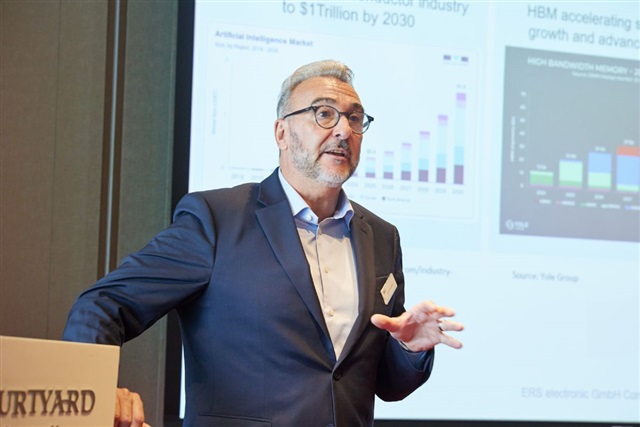
Laurent Giai-Miniet, CEO of ERS, appears in the image above, underscoring growing industry focus on thermal and test considerations that are pivotal to reliable, high-yield fan-out packaging.