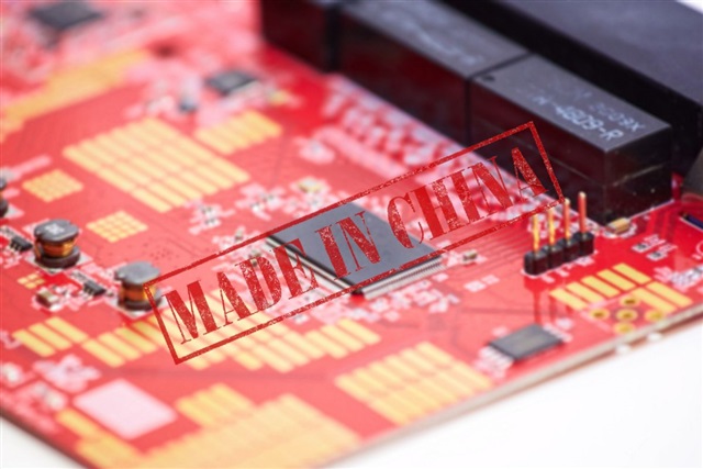
China’s EUV Gap Keeps Semiconductor Catch-Up in Check Despite Progress in Chip Packaging
China’s semiconductor industry is moving quickly, but one major obstacle continues to define the limits of its progress: access to extreme ultraviolet lithography, better known as EUV. As the United States tightens export controls on advanced chipmaking equipment, China is being forced to find alternative ways to improve chip performance without relying on the world’s most advanced manufacturing tools.
The central question is whether China can narrow the semiconductor gap by focusing on mature chip nodes, advanced packaging, and domestic equipment development. These areas are important, and China has made visible progress in them. However, they are not a complete substitute for leading-edge EUV-based manufacturing, especially when it comes to producing the most advanced processors used in artificial intelligence, high-performance computing, premium smartphones, and next-generation data centers.
EUV lithography is one of the most difficult technologies in the global chip industry. It allows manufacturers to print extremely tiny circuit patterns on silicon wafers, making it possible to produce chips with higher transistor density, better power efficiency, and stronger performance. Without EUV tools, it becomes much harder to compete at the most advanced process nodes, where global leaders are pushing toward ever-smaller and more efficient designs.
A key reason this technology is so difficult to replicate is the precision required across the entire supply chain. EUV systems rely on ultra-advanced optics, light sources, mirrors, vacuum systems, and software working together at an extraordinary level of accuracy. German optics specialist Zeiss plays a critical role in this ecosystem, supplying highly complex optical components needed for EUV lithography machines. Recreating this capability domestically is not simply a matter of funding; it requires years of accumulated expertise, specialized manufacturing, and an extremely mature supply network.
Because of these restrictions, China has been leaning more heavily on mature semiconductor nodes. These older process technologies remain highly valuable for a wide range of industries, including electric vehicles, consumer electronics, industrial equipment, power management chips, communications hardware, and home appliances. In fact, demand for mature-node chips remains strong worldwide, and China has the capacity to become even more influential in this segment.
Advanced packaging is another area where China sees an opportunity. Instead of shrinking transistors through cutting-edge lithography, advanced packaging improves performance by placing multiple chips closer together, improving bandwidth, reducing latency, and increasing efficiency. Chiplet designs, 2.5D packaging, and 3D stacking can help manufacturers build more powerful systems even when they cannot access the most advanced fabrication nodes.
This approach can deliver real gains, especially for certain AI accelerators, servers, and custom computing products. However, advanced packaging cannot fully erase the disadvantage of being behind in leading-edge process technology. Packaging can improve how chips communicate and work together, but the performance and efficiency of each individual chip still depend heavily on the node used to manufacture it.
That is why China’s semiconductor ambitions face a complicated path. Mature nodes can strengthen domestic supply chains and reduce dependence on foreign suppliers in many important industries. Advanced packaging can help stretch the capabilities of existing manufacturing processes. Domestic equipment development can gradually reduce exposure to export restrictions. But without EUV lithography, catching up at the very top end of the chip market remains extremely difficult.
The global semiconductor race is no longer only about who can build the smallest transistor. It is also about supply chain resilience, packaging innovation, materials science, design tools, and manufacturing scale. China is investing across all of these areas, and its progress should not be underestimated. Still, the EUV gap remains one of the biggest barriers preventing the country from matching the most advanced chipmakers.
For now, export controls are shaping the direction of China’s chip strategy. Instead of competing directly at the cutting edge, China is likely to expand its strength in mature nodes, improve domestic production tools, and accelerate advanced packaging development. This could make the country more self-sufficient in many parts of the semiconductor market, even if it remains behind in the most advanced logic chips.
The result is a semiconductor industry that is advancing, but unevenly. China may continue to gain ground in areas where EUV is not essential, while facing major challenges in sectors that demand the most advanced chip manufacturing. Until it can overcome the EUV bottleneck, the gap in leading-edge semiconductors is likely to remain a defining feature of the global technology landscape.