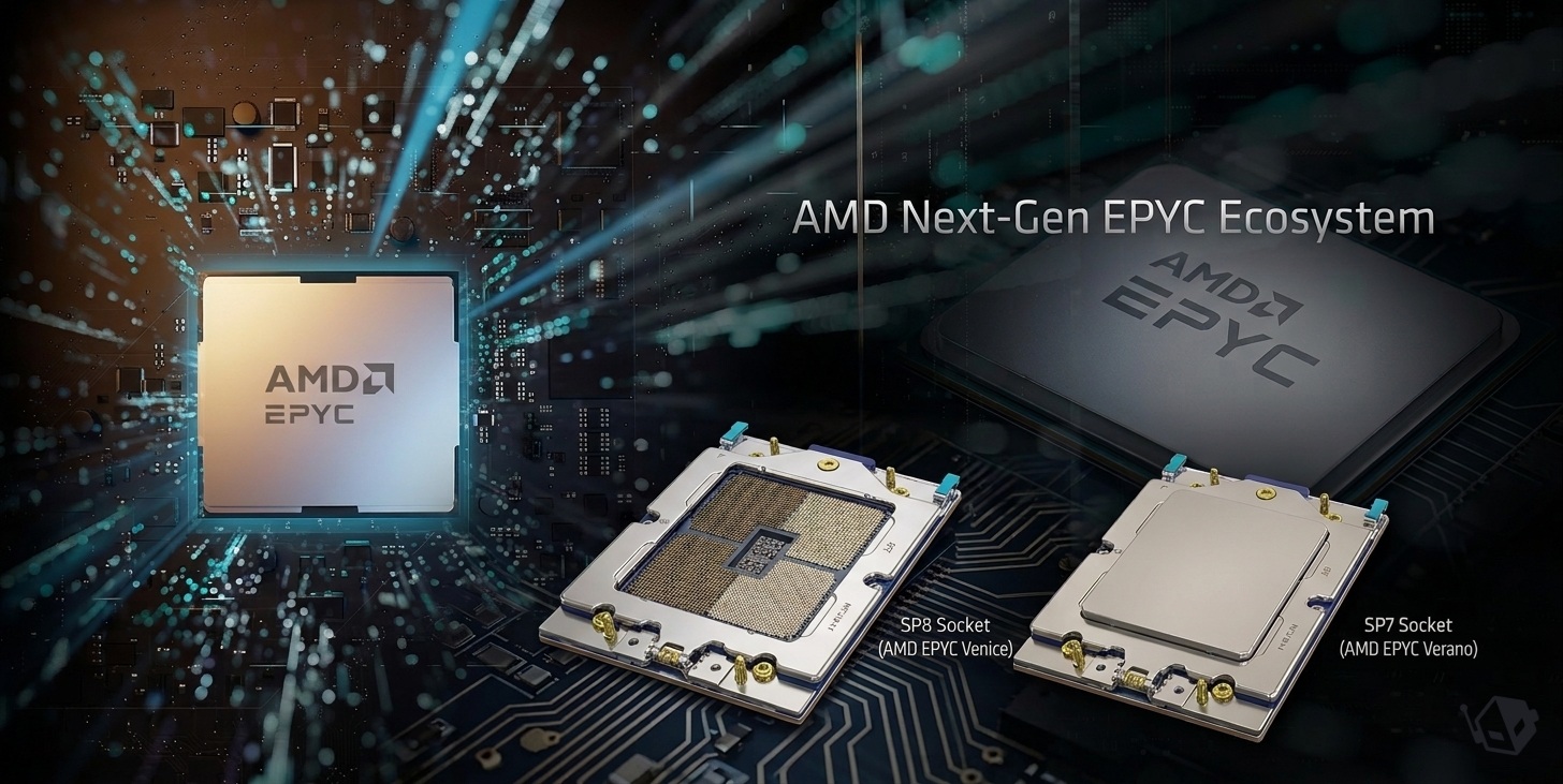
AMD is preparing a major platform refresh for its next wave of EPYC server processors, and newly surfaced details point to two brand-new CPU sockets: SP7 and SP8. Built to support the Zen 6-based EPYC Venice and EPYC Verano families, these sockets are physically larger than the current generation—an early sign of higher compute density, more power delivery, and expanded I/O that modern data centers are demanding.
EPYC Venice, previously announced as AMD’s high-end next-gen server CPU line, is expected to arrive in 2026. It includes ultra-dense Zen 6C variants scaling as high as 256 cores. EPYC Verano, positioned as a more cost-effective Zen 6 option, is targeted for 2027. To accommodate these chips, AMD is moving to updated server platforms with bigger sockets and more ambitious memory and connectivity targets.
Let’s start with SP7, the successor directionally aligned with today’s SP5 ecosystem used by EPYC Genoa and Turin. The SP7 socket is reported at 123.6 x 100.6mm, roughly 12% larger than SP5. The physical structure maintains a multi-part design with a socket retention mechanism (SRM) on top, a carrier board, the motherboard housing, and a backplate. In practical terms, that typically means better mechanical stability, refined load distribution, and room for more contacts—key when CPUs are pushing higher core counts, faster memory, and significantly more power.
SP8 is designed for EPYC Verano and comes in at 123.9 x 80.9mm. While smaller than SP7, it’s still about 7% larger than the SP6 generation. One notable platform change is that SP8 is expected to use the SRM load mechanism as well, whereas SP6 relied on a different actuation approach (SAM). That standardization can simplify server design strategies for OEMs while still allowing AMD to differentiate platforms by performance, memory channels, and I/O capabilities.
On the platform side, SP7 is shaping up as the high-end option for enterprise and hyperscale deployments. The headline feature is memory bandwidth: up to 16-channel DDR5 with ECC support, with speeds listed up to 8000 MT/s. It also references MRDIMM support reaching as high as 12,800 MT/s in 1DPC configurations, along with broader DIMM compatibility that includes RDIMM, 3DS RDIMM, MRDIMM, and tall DIMM solutions. AMD is also expected to support multiple memory interleave modes, ranging from single-channel interleave options through higher multi-channel configurations, giving system builders flexibility to optimize for capacity, bandwidth, or latency.
I/O is equally aggressive. The SP7 2P (dual-socket) platform is expected to provide up to 128 PCIe Gen 6 lanes, plus up to 16 additional “bonus” PCIe Gen 4 lanes. For 1P (single-socket) systems, the figures shift to up to 96 PCIe Gen 6 lanes and 8 PCIe Gen 4 lanes. PCIe Gen 6 is a major leap for next-generation networking, storage, and accelerator connectivity, especially as data centers scale out with faster fabrics and more GPUs. The platform is also mentioned as supporting Smart Data Cache Injection (SDCI).
SP8, despite being positioned as an entry-level platform compared to SP7, isn’t simply a cut-down design. Memory support is said to remain similar in terms of DIMM types and speed capabilities, but limited to 8-channel configurations instead of 16-channel. The surprising part is I/O: SP8 is reported to offer even more PCIe Gen 6 lanes than SP7. Numbers cited include up to 192 PCIe Gen 6 lanes (plus 16 PCIe Gen 4 lanes) for 2P, and up to 128 PCIe Gen 6 lanes (plus 8 PCIe Gen 4 lanes) for 1P. If accurate, that could make SP8 particularly attractive for systems that prioritize connectivity—think storage-dense servers, networking-heavy nodes, or accelerator-rich designs—while staying in a more cost-conscious CPU tier.
The CPU roadmap details help explain why AMD is scaling the platform like this. EPYC Venice in Zen 6C “dense” configurations is expected to reach up to 32 cores per CCD across as many as 8 CCDs, landing at the widely discussed 256-core ceiling. Cache scaling looks just as dramatic: 128MB of L3 cache per CCD, totaling 1024MB (1GB) L3 on a full 8-CCD configuration. That kind of cache capacity can significantly improve performance in data analytics, large in-memory workloads, and cloud multi-tenant environments that benefit from reduced memory trips.
The package also includes two I/O dies, each expected to handle PCIe Gen 6 and CXL 3.1, along with DDR5-8000 memory support, Infinity Fabric improvements, and security features such as a secure processor. One detail to watch: some diagrams suggest MRDIMM speeds may top out at 10,400 MT/s in certain configurations, even though higher figures are also mentioned elsewhere. That discrepancy could come down to platform validation targets, DIMM availability, or differences between early specs and final shipping support.
For standard Zen 6 (non-dense) EPYC Venice and Verano parts, the outlined configuration points to 12 cores per CCD across 8 CCDs, resulting in up to 96 cores and 192 threads—matching today’s top mainstream core count tier in the EPYC lineup. Cache per CCD is expected to rise to 48MB L3, a 50% increase over the 32MB per CCD commonly associated with Zen 5-based designs. Even without pushing core counts higher, those cache and platform upgrades can translate into real gains across virtualization, databases, and mixed enterprise workloads.
Power is climbing as well, reflecting the shift toward more cores, higher clocks, faster DDR5, and PCIe Gen 6 signaling. SP7-based CPUs are rumored to reach around 600W TDP, up from roughly 400W in the Zen 5 era. SP8 parts are tagged in the 350W to 400W range. That implies server vendors will be pairing these platforms with more robust VRM designs and more capable cooling solutions—especially in dense rack deployments.
Taken together, SP7 and SP8 underline AMD’s next step in the data center CPU race: more cores, more cache, faster memory, and a big push into PCIe Gen 6 and CXL 3.1-era infrastructure. With EPYC Venice expected in 2026 and EPYC Verano following in 2027, the next couple of years are shaping up to be a major transition period for server buyers planning new platforms, refresh cycles, and next-gen workloads.