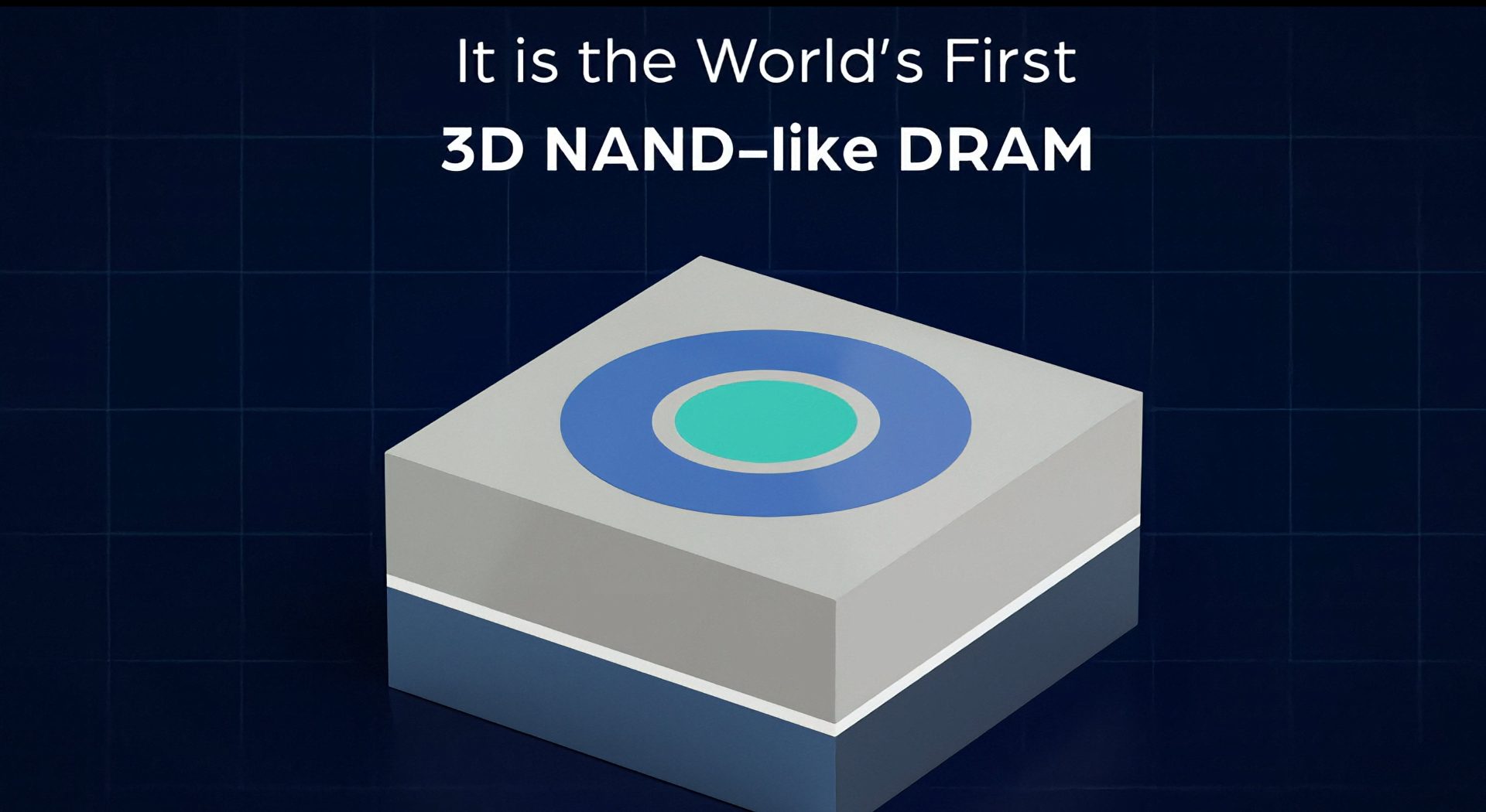
Imagine DRAM capacity scaling the way 3D NAND did: instead of relying on big gains from shrinking nodes, you add more layers to pack in far more memory per chip. That’s the idea behind 3D X-DRAM, a new approach from U.S.-based NEO Semiconductor that targets one of the biggest pain points in modern computing: the growing DRAM capacity and bandwidth demands driven by AI and high-performance computing.
NEO Semiconductor first introduced 3D X-DRAM in 2023 as a way to tackle the DRAM bottleneck by using a NAND-like 3D architecture. Rather than stacking multiple separate DRAM dies the way High-Bandwidth Memory (HBM) typically does, 3D X-DRAM aims for a monolithic-like design within a single die, building DRAM in many layers using processes similar to existing 3D NAND manufacturing. The promise is straightforward: significantly higher density, strong performance, and a path that could be more manufacturing-friendly than complex stacked-memory solutions.
A key part of the concept is a set of new memory cell designs intended to serve different markets and workloads. NEO has discussed multiple cell types for 3D X-DRAM-based products, including:
1T1C (one transistor, one capacitor) – Designed as a high-density DRAM option that aligns with mainstream DRAM roadmaps and can fit alongside existing directions in the broader memory ecosystem.
3T0C (three transistors, zero capacitor) – Tuned for current-sensing operations, positioning it as a good match for AI-oriented tasks and in-memory computing approaches.
1T0C (one transistor, zero capacitor) – A floating-body cell structure aimed at high-density DRAM use cases, including hybrid memory concepts and logic-related architectures.
NEO has previously stated that its 3D X-DRAM approach could reach densities up to 512Gb, representing a claimed 10x density improvement compared to traditional DRAM, while also targeting cost-effective, high-yield production. If those goals translate into real-world products at scale, it could materially change how memory is provisioned for AI training, inference, and next-generation servers.
One of the more attention-grabbing claims around the technology is retention and power efficiency. Using IGZO channel technology, NEO’s simulations indicated retention times as high as 450 seconds for the 1T1C and 3T0C designs, which would dramatically reduce the need for refresh operations and, in turn, lower power use. The company also highlighted TCAD simulations showing fast read/write performance around 10 nanoseconds along with that long retention behavior.
Beyond cell design, the pitch includes practical manufacturing and system-level benefits. NEO says 3D X-DRAM can be produced using a modified 3D NAND process with minimal changes, helping it scale and potentially integrate faster with established semiconductor manufacturing infrastructure. It also points to array architectures designed for hybrid bonding, aiming to increase bandwidth while cutting power—an increasingly critical balance for AI accelerators and data center deployments where energy efficiency is now a first-class constraint.
The comparison to HBM is important in the AI and HPC conversation. HBM delivers excellent bandwidth and is widely used on leading accelerators, but it’s also expensive, difficult to produce at scale, and typically requires extensive testing and verification before deployment on high-value server hardware. Conventional DRAM is generally easier to manufacture and validate. 3D X-DRAM is positioned as an approach that can close the density and bandwidth gap while avoiding some of the complexity associated with multi-die stacking.
Now, the project appears to be taking a concrete step forward. NEO Semiconductor has announced it demonstrated a proof-of-concept (POC) for 3D X-DRAM and secured investment to continue advancing development. With its POC test chips, the company says it has shown the ability to manufacture 3D X-DRAM using existing 3D NAND infrastructure—building multiple DRAM layers as part of the die approach, rather than relying on a stacked arrangement similar to HBM.
Early POC test results shared for these chips include:
Read/write latency: under 10 ns
Data retention: over 1 second at 85°C (claimed 15x better than the 64 ms JEDEC standard)
Bit-line disturbance: over 1 second at 85°C
Word-line disturbance: over 1 second at 85°C
Endurance: over 10¹⁴ cycles
While these figures come from early test chips rather than mass-produced memory for shipping systems, they underline why the industry is watching layered DRAM concepts closely. AI models continue to push memory requirements—not just in raw capacity, but also in bandwidth, efficiency, and total cost at scale. As a result, advanced DRAM architectures are increasingly seen as necessary for the next wave of servers, accelerators, and edge computing platforms.
NEO isn’t alone in pursuing a rethink of DRAM structure. Intel is also preparing a similar concept known as ZAM (Z-Angle Memory). At the moment, neither approach is in production, and widespread deployment is still some distance away. Still, with continued progress and ongoing investment, there’s a realistic possibility that new 3D DRAM-style technologies could begin influencing the server and AI hardware landscape within this decade.